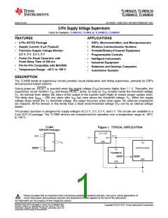
TLV809J25, TLV809L30
TLV809K33, TLV809I50
www.ti.com
SLVSA03C –JUNE 2010–REVISED FEBRUARY 2012
THERMAL INFORMATION
TLV809
DBV
TLV809
DBZ
THERMAL METRIC(1)
UNITS
3 PINS
242.1
213.0
123.4
45.7
3 PINS
286.9
105.6
124.4
25.8
θJA
Junction-to-ambient thermal resistance
Junction-to-case (top) thermal resistance
Junction-to-board thermal resistance
θJCtop
θJB
°C/W
ψJT
Junction-to-top characterization parameter
Junction-to-board characterization parameter
Junction-to-case (bottom) thermal resistance
ψJB
130.9
—
107.9
—
θJCbot
(1) For more information about traditional and new thermal metrics, see the IC Package Thermal Metrics application report, SPRA953.
RECOMMENDED OPERATING CONDITIONS
At specified temperature range (unless otherwise noted).
MIN
2
MAX
6
UNIT
V
VDD
TA
Supply voltage
Operating free-air temperature range
–40
+85
°C
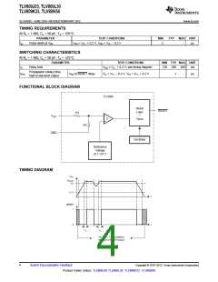
ELECTRICAL CHARACTERISTICS
Over recommended operating free-air temperature range (unless otherwise noted).
PARAMETER
TEST CONDITIONS
MIN
VDD – 0.2
VDD – 0.4
VDD – 0.4
TYP
MAX UNIT
VDD = 2.5 V to 6 V, IOH = –500 µA
VOH
High-level output voltage
VDD = 3.3 V,
VDD = 6 V,
IOH = –2 mA
IOH = –4 mA
IOH = 500 µA
IOH = 2 mA
IOH = 4 mA
IOL = 50 µA
V
VDD = 2 V to 6 V,
VDD = 3.3 V,
VDD = 6 V,
0.2
VOL
Low-level output voltage
Power-up reset voltage(1)
0.4
0.4
V
V
V
DD ≥ 1.1 V,
0.2
TLV809J25
TLV809L30
TLV809K33
TLV809I50
TLV809J25
TLV809L30
TLV809K33
TLV809I50
2.20
2.58
2.87
4.45
2.25
2.64
2.93
4.55
30
2.30
2.70
2.99
4.65
Negative-going input
threshold voltage(2)
VIT–
TA = –40°C to 85°C
v
35
Vhys
Hysteresis
mV
40
60
VDD = 2 V,
Output unconnected
Output unconnected
9
12
25
IDD
Ci
Supply current
µA
pF
VDD = 6 V,
20
Input capacitance
VI = 0 V to VDD
5
(1) The lowest supply voltage at which RESET becomes active. tr, VDD ≥ 15 ms/V.
(2) To ensure best stability of the threshold voltage, a bypass capacitor ( 0.1-µF ceramic) should be placed near the supply terminals.
Copyright © 2010–2012, Texas Instruments Incorporated
Submit Documentation Feedback
3
Product Folder Link(s): TLV809J25 TLV809L30 TLV809K33 TLV809I50

 TI [ TEXAS INSTRUMENTS ]