TLV809J25, TLV809L30
TLV809K33, TLV809I50
SLVSA03C –JUNE 2010–REVISED FEBRUARY 2012
www.ti.com
This integrated circuit can be damaged by ESD. Texas Instruments recommends that all integrated circuits be handled with
appropriate precautions. Failure to observe proper handling and installation procedures can cause damage.
ESD damage can range from subtle performance degradation to complete device failure. Precision integrated circuits may be more
susceptible to damage because very small parametric changes could cause the device not to meet its published specifications.
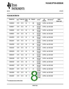
PACKAGE/ORDERING INFORMATION(1)
SPECIFIED
THRESHOLD
VOLTAGE
PACKAGE-
LEAD
PACKAGE
DESIGNATOR
OPERATING
TEMPERATURE
PACKAGE
MARKING
ORDERING
INFORMATION
TRANSPORT MEDIA,
QUANTITY
PRODUCT
TLV809J25DBVR
TLV809J25DBVT
TLV809J25DBZR
TLV809J25DBZT
TLV809L30DBVR
TLV809L30DBVT
TLV809L30DBZR
TLV809L30DBZT
TLV809K33DBVR
TLV809K33DBVT
TLV809K33DBZR
TLV809K33DBZT
TLV809I50DBVR
TLV809I50DBVT
TLV809I50DBZR
TLV809I50DBZT
Tape and Reel, 3000
Tape and Reel, 250
Tape and Reel, 3000
Tape and Reel, 250
Tape and Reel, 3000
Tape and Reel, 250
Tape and Reel, 3000
Tape and Reel, 250
Tape and Reel, 3000
Tape and Reel, 250
Tape and Reel, 3000
Tape and Reel, 250
Tape and Reel, 3000
Tape and Reel, 250
Tape and Reel, 3000
Tape and Reel, 250
DBV
DBZ
DBV
DBZ
DBV
DBZ
DBV
DBZ
–40°C to +85°C
–40°C to +85°C
–40°C to +85°C
–40°C to +85°C
–40°C to +85°C
–40°C to +85°C
–40°C to +85°C
–40°C to +85°C
VTCI
BCMT
VTXI
TLV809J25
2.25 V
2.64 V
2.93 V
4.55 V
SOT23-3
SOT23-3
SOT23-3
SOT23-3
TLV809L30
TLV809K33
TLV809I50
BCMZ
VTRI
BCMX
VTBI
BCMV
(1) For the most current package and ordering information, see the Package Option Addendum at the end of this data sheet, or visit the
device product folder at www.ti.com.
ABSOLUTE MAXIMUM RATINGS(1)
Over operating free-air temperature range (unless otherwise noted) .
VALUE
UNIT
V
VDD
Supply voltage(2)
7
–0.3 to 7
5
All other pins(2)
V
IOL
IOH
IIK
Maximum low output current
Maximum high output current
Input clamp current (VI < 0 or VI > VDD
mA
mA
mA
mA
°C
–5
)
±20
IOK
TA
Output clamp current (VO < 0 or VO > VDD
Operating free-air temperature range
Storage temperature range
)
±20
–40 to +85
–65 to +150
+260
Tstg
°C
Soldering temperature
°C
(1) Stresses beyond those listed under Absolute Maximum Ratings may cause permanent damage to the device. These are stress ratings
only, and functional operation of the device at these or any other conditions beyond those indicated under Recommended Operating
Conditions is not implied. Exposure to absolute-maximum-rated conditions for extended periods may affect device reliability.
(2) All voltage values are with respect to GND. For reliable operation the device should not be operated at 7 V for more than t = 1000h
continuously
2
Submit Documentation Feedback
Copyright © 2010–2012, Texas Instruments Incorporated
Product Folder Link(s): TLV809J25 TLV809L30 TLV809K33 TLV809I50

 TI [ TEXAS INSTRUMENTS ]