TLV61220
SLVSB53 –MAY 2012
www.ti.com
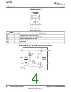
PIN ASSIGNMENTS
DBV PACKAGE
TOP VIEW
VBAT VOUT FB
6
1
5
4
3
A B C
2
SW
GND EN
Terminal Functions
TERMINAL
I/O
DESCRIPTION
NAME
EN
NO.
3
4
2
1
6
5
I
I
Enable input (VBAT enabled, GND disabled)
Voltage feedback for programming the output voltage
IC ground connection for logic and power
Boost and rectifying switch input
Supply voltage
FB
GND
SW
I
I
VBAT
VOUT
O
Boost converter output
FUNCTIONAL BLOCK DIAGRAM (ADJUSTABLE VERSION)
VOUT
SW
VOUT
VIN
Gate
Driver
Start Up
VBAT
Current
Sensor
Device
Control
FB
EN
VREF
GND
4
Submit Documentation Feedback
Copyright © 2012, Texas Instruments Incorporated
Product Folder Link(s): TLV61220

 TI [ TEXAS INSTRUMENTS ]