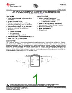
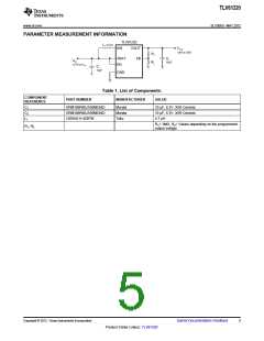
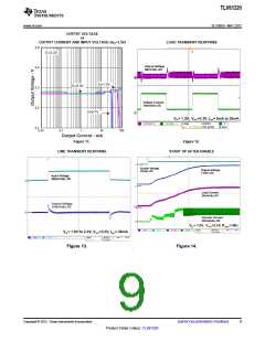
TLV61220
www.ti.com
SLVSB53 –MAY 2012
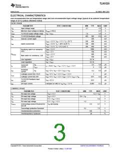
ELECTRICAL CHARACTERISTICS
over recommended free-air temperature range and over recommended input voltage range (typical at an ambient temperature
range of 25°C) (unless otherwise noted)
DC/DC STAGE
PARAMETER
TEST CONDITIONS
MIN
TYP
MAX
5.5
UNIT
V
VIN
Input voltage range
0.7
VIN
Minimum input voltage at startup
TLV61220 output voltage range
TLV61220 feedback voltage
Inductor current ripple
R
Load ≥ 150 Ω
0.7
V
VOUT
VFB
ILH
VIN < VOUT
1.8
5.5
V
483
500
200
400
400
400
1000
700
600
550
0.5 %
0.5 %
0.5
513
mV
mA
mA
mA
mA
mΩ
mΩ
mΩ
mΩ
VOUT = 3.3 V, VIN = 1.2 V, TA = 25 °C
VOUT = 3.3 V, TA = -40°C to 85 °C
VOUT = 3.3 V, TA = 0°C to 85 °C
VOUT = 3.3 V
220
180
200
ISW
switch current limit
Rectifying switch on resistance,
HSD
VOUT = 5 V
RDS(on)
VOUT = 3.3 V
Main switch on resistance, LSD
VOUT = 5 V
Line regulation
Load regulation
VIN < VOUT
VIN < VOUT
VIN
0.9
7.5
μA
μA
Quiescent
current
IQ
IO = 0 mA, VEN = VIN = 1.2 V, VOUT = 3.3 V
VOUT
5
Shutdown
current
ISD
ILKG
IFB
IEN
VIN
VEN = 0 V, VIN = 1.2 V, VOUT ≥ VIN
0.2
0.5
μA
Leakage current into VOUT
Leakage current into SW
VEN = 0 V, VIN = 1.2 V, VOUT = 3.3 V
1
μA
μA
VEN = 0 V, VIN = 1.2 V, VSW = 1.2 V, VOUT ≥ VIN
0.01
0.2
TLV61220 Feedback input
current
VFB = 0.5 V
0.01
μA
μA
EN input current
Clamped on GND or VIN (VIN < 1.5 V)
0.005
0.1
CONTROL STAGE
PARAMETER
TEST CONDITIONS
MIN
TYP
MAX
UNIT
VIL
EN input low voltage
EN input high voltage
EN input low voltage
EN input high voltage
V
IN ≤ 1.5 V
IN ≤ 1.5 V
0.2 × VIN
V
V
V
V
V
VIH
V
0.8 × VIN
1.2
VIL
5 V > VIN > 1.5 V
5 V > VIN > 1.5 V
VIN decreasing
0.4
VIH
VUVLO
Undervoltage lockout threshold for
turn off
0.5
0.7
7.5
Overvoltage protection threshold
Overtemperature protection
Overtemperature hysteresis
5.5
V
140
20
°C
°C
Copyright © 2012, Texas Instruments Incorporated
Submit Documentation Feedback
3
Product Folder Link(s): TLV61220

 TI [ TEXAS INSTRUMENTS ]