TLV61220
SLVSB53 –MAY 2012
www.ti.com
These devices have limited built-in ESD protection. The leads should be shorted together or the device placed in conductive foam
during storage or handling to prevent electrostatic damage to the MOS gates.
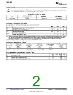
AVAILABLE DEVICE OPTIONS
OUTPUT VOLTAGE
TA
PACKAGE
PART NUMBER
DC/DC
–40°C to 85°C
Adjustable
6-Pin SOT-23
TLV61220DBV
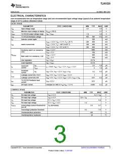
ABSOLUTE MAXIMUM RATINGS
over operating free-air temperature range (unless otherwise noted)(1)
MIN
– 0.3 to
–40
MAX
7.5
150
150
2
UNIT
V
VIN
TJ
Input voltage range on VBAT, SW, VOUT, EN, FB
Operating junction temperature range
Storage temperature range
°C
Tstg
–65
°C
(2)
Human Body Model (HBM)
kV
kV
ESD
Charged Device Model (CDM)(2)
1.5
(1) Stresses beyond those listed under Absolute Maximum Ratings may cause permanent damage to the device. These are stress ratings
only, and functional operation of the device at these or any other conditions beyond those indicated under Recommended Operating
Conditions is not implied. Exposure to absolute-maximum-rated conditions for extended periods may affect device reliability.
(2) ESD testing is performed according to the respective JESD22 JEDEC standard.
DISSIPATION RATINGS TABLE
THERMAL
THERMAL
RESISTANCE
ΘJB
THERMAL
RESISTANCE
ΘJC
DERATING FACTOR
ABOVE
POWER RATING
PACKAGE
RESISTANCE
TA ≤ 25°C
(1)
ΘJA
TA = 25°C
DBV
130 °C/W
27 °C/W
41 °C/W
769 mW
7.7 mW/°C
(1) Thermal ratings are determined assuming a high K PCB design according to JEDEC standard JESD51-7.
RECOMMENDED OPERATING CONDITIONS
MIN
NOM
MAX
5.5
UNIT
V
VIN
TA
TJ
Supply voltage at VIN
0.7
–40
–40
Operating free air temperature range
Operating virtual junction temperature range
85
°C
125
°C
2
Submit Documentation Feedback
Copyright © 2012, Texas Instruments Incorporated
Product Folder Link(s): TLV61220

 TI [ TEXAS INSTRUMENTS ]