TLV3501-Q1
www.ti.com
SBOS533A –SEPTEMBER 2010–REVISED SEPTEMBER 2010
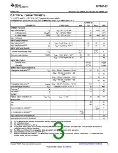
ELECTRICAL CHARACTERISTICS
TA = +25°C and VS = +2.7 V to +5.5 V (unless otherwise noted).
Boldface limits apply over the specified temperature range, TA = −40°C to +125°C.
TLV3501-Q1
TYP
PARAMETER
CONDITIONS
MIN
MAX
UNIT
OFFSET VOLTAGE
Input offset voltage(1)
VOS
dVOS/dT
PSRR
VCM = 0 V, IO = 0 mA
TA = −40°C to +125°C
VS = 2.7 V to 5.5 V
±1
±5
±6.5
mV
mV/°C
mV/V
mV
vs Temperature
vs Power supply
100
6
400
Input hysteresis
INPUT BIAS CURRENT
Input bias current(2)
Input offset current(2)(3)
IB
VCM = VCC/2, ΔVIN= ±5.5 V
VCM = VCC/2ΔVIN= ±5.5 V
±2
±2
±10
pA
pA
IOS
±10
INPUT VOLTAGE RANGE
(V–) −
0.2 V
(V+) +
0.2 V
Common-mode voltage range
Common-mode rejection
VCM
V
CMRR
VCM = −0.2 V to (V+) + 0.2V
VCM = −0.2 V to (V+) + 0.2V
57
70
dB
55
dB
INPUT IMPEDANCE
Common-mode
1013 || 2
1013 || 4
Ω || pF
Ω || pF
Differential
SWITCHING CHARACTERISTICS
Propagation delay time(2)(4)
T(pd) ΔVIN = 100 mV, Overdrive = 20 mV
4.5
7.5
6.4
ns
ns
ns
ns
ΔVIN = 100 mV, Overdrive = 20
7
10
12
mV
ΔVIN = 100 mV, Overdrive = 5 mV
ΔVIN = 100 mV, Overdrive = 20
mV
Propagation delay skew(5)
Maximum toggle frequency
Rise time(6)
Δt(SKEW) ΔVIN = 100 mV, Overdrive = 20 mV
0.5
80
ns
MHz
ns
fMAX
tR
Overdrive = 50 mV, VS = 5 V
1.5
1.5
Fall time(6)
tF
ns
OUTPUT
Voltage output swing from rail
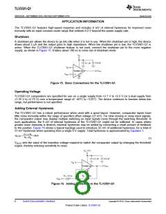
SHUTDOWN
VOH, VOL
IOUT = ±1 mA
30
50
mV
tOFF
30
ns
ns
tON
100
(V+) −
1.7V
VH (comparator is enabled)(7)
VL (comparator is disabled)(7)
V
V
(V+) −
0.9V
Input bias current of Shutdown pin
IQSD (quiescent current in shutdown)
2
2
pA
mA
(1) VOS is defined as the average of the positive and the negative switching thresholds.
(2) Not production tested.
(3) The difference between IB+ and IB−
.
(4) Propagation delay cannot be accurately measured with low overdrive on automatic test equipment. This parameter is ensured by
characterization at 100-mV overdrive.
(5) The difference between the propagation delay going high and the propagation delay going low.
(6) Measured between 10% of VS and 90% of VS.
(7) When the shutdown pin is within 0.9 V of the most positive supply, the part is disabled. When it is more than 1.7 V below the most
positive supply, the part is enabled.
Copyright © 2010, Texas Instruments Incorporated
Submit Documentation Feedback
3
Product Folder Link(s): TLV3501-Q1

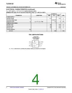
 TI [ TEXAS INSTRUMENTS ]