Application examples
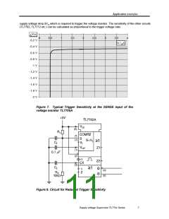
In applications where this performance is not required, sensitivity can be reduced by placing an R-C filter in
front of SENSE input. To avoid a unacceptable change of the threshold voltage of circuits with a fixed
threshold voltage (TL7705, TL7709, TL7712, TL7715) the value of the resistor should be a few 10W only.
In application like this it may be better to use the TL7702A. With this circuit the threshold voltage can be
set to the desired value by a high impedance voltage monitor. A small filter capacitor C at the SENSE
f
input reduces the trigger sensitivity (figure 8).
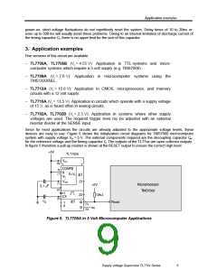
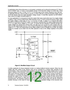
In some applications it is necessary to keep the output of the reset circuit active even if no supply voltage
is applied. Under normal conditions the output transistor of the TL77xxA is turned off (inactive state), when
the supply voltage is lower than 3V (Vcc > 1 V for the TL77xxB). In figure 9 a P-channel field effect
transistor is connected to theRESET output. This transistor conducts when the supply voltage drops below
3 V i.e. at a gate source voltage of -3V or less. To ensure that the transistor is switched off when the
supply voltage has reached the nominal value, the gate has to be at least 6V more positive than the
source (or the required high level e.g. 2.4V). In figure 9 therefore the voltage monitor is supplied by supply
voltage of 12 V. Since the requirements for this supply voltage in terms of stability are not high, this supply
voltage for example can be taken from the filter capacitor in front of the voltage regulator in the power
supply.
Figure 9. Modified Output Circuit
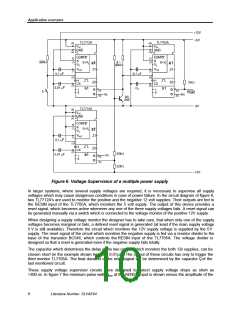
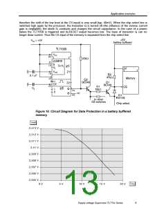
A further application for these integrated circuits is in battery-buffered memory systems. When the line
voltage fails, the content of the memory must not be corrupted by a random write operation of the
microcomputer. These uncontrolled write operations may take place at low supply voltage even if a reset
signal is applied to the processor. Generally, it is sufficient to switch the chip select line into the inactive
state (some memories require that the write line also be disabled). A switch, which consists of transistor Q
1
and diode D1, is inserted into the chip select line of the memory. Under normal operation (line voltage
present) the output of the TL7705B is turned off (high); the transistor Q draws its base current from
1
transistor Q2 and resistor R1. When the chip select line is switched from high to low by the supervising
microprocessor, the transistor conducts and the CS input of the memory goes low and the memory is
enabled. Because of the small DC load of the resistor R, the saturation voltage of the transistor (and
2
8
Literature Number: SLVAE04

 TI [ TEXAS INSTRUMENTS ]