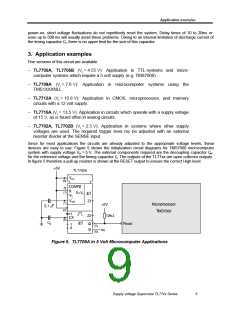
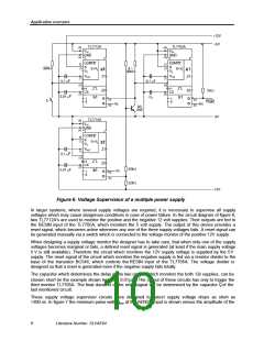
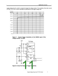
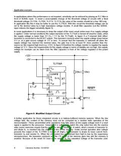
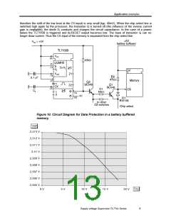
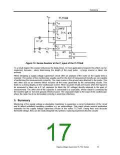
Application examples
therefore the shift of the low level at the CS input) is very small (typ. 40mV). When the chip select line is
switched high again by the processor, the transistor Q is turned off (the influence of the inverse current
1
gain is negligible); the diode D conducts and charges the circuit capacitance. In the case of a power-
1
failure the TL7705B is triggered and its RESET output becomes low. The base of transistor Q can no
1
longer draw current. Thus the CS input of the memory is separated from the chip select line.
Figure 10. Circuit Diagram for Data Protection in a battery buffered
memory
Vref
2,513 V
2,512 V
2,511 V
2,51 V
2,509 V
2,508 V
2,507 V
2,506 V
2,505 V
Vcc
0 V
5 V
10 V
15 V
20 V
Supply voltage Supervisor TL77xx Series
9

 TI [ TEXAS INSTRUMENTS ]