THS4531
SLOS358B –SEPTEMBER 2011–REVISED MARCH 2012
www.ti.com
Low Power Applications and the Effects of Resistor Values on Bandwidth
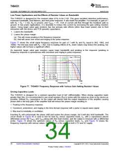
The THS4531 is designed for the nominal value of RF to be 2 kΩ. This gives excellent distortion performance,
maximum bandwidth, best flatness, and best pulse response. It also loads the amplifier. For example; in gain of 1
with RF = RG = 2 kΩ, RG to ground, and VOUT+ = 4V, 1mA of current will flow through the feedback path to
ground. In low power applications, it is desirable to reduce this current by increasing the gain setting resistors
values. Using larger value gain resistors has two primary side effects (other than lower power) due to their
interaction with the device and PCB parasitic capacitance:
1. Lowers the bandwidth.
2. Lowers the phase margin
(a) This will cause peaking in the frequency response.
(b) And will cause over shoot and ringing in the pulse response.
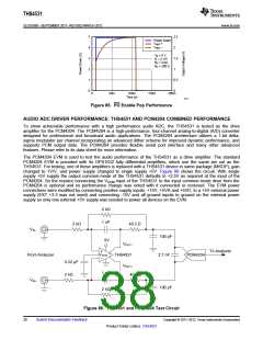
Figure 77 shows the small signal frequency response for gain of 1 with RF and RG equal to 2kΩ, 10kΩ, and
100kΩ. The test was done with RL = 2kΩ. Due to loading effects of RL, lower values may reduce the peaking, but
higher values will not have a significant effect.
As expected, larger value gain resistors cause lower bandwidth and peaking in the response (peaking in
frequency response is synonymous with overshoot and ringing in pulse response).
9
VOUT = 100 mVPP
6
3
0
−3
−6
−9
−12
RF = 2 kΩ
RF = 10 kΩ
RF = 100 kΩ
−15
−18
−21
100k
1M
10M
100M
Frequency (Hz)
G067
Figure 77. THS4531 Frequency Response with Various Gain Setting Resistor Values
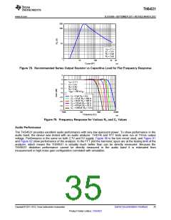
Driving Capacitive Loads
The THS4531 is designed for a nominal capacitive load of 2pF (differentially). When driving capacitive loads
greater than this, it is recommended to use small resisters (RO) in series with the output as close to the device as
possible. Without RO, capacitance on the output will interact with the output impedance of the amplifier causing
phase shift in the loop gain of the amplifier that will reduce the phase margin resulting in:
1. Peaking in the frequency response.
2. Overshoot, undershoot, and ringing in the time domain response with a pulse or square-wave signal.
3. May lead to instability or oscillation.
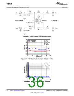
Inserting RO will compensate the phase shift and restore the phase margin, but it will also limit bandwidth. The
circuit shown in Figure 69 is used to test for best RO versus capacitive loads, CL, with a capacitance placed
differential across the VOUT+ and VOUT-along with 2kΩ load resistor, and the output is measure with a differential
probe. Figure 78 shows the optimum values of RO versus capacitive loads, CL, and Figure 79 shows the
frequency response with various values. Performance is the same on both 2.7V and 5V supply.
34
Submit Documentation Feedback
Copyright © 2011–2012, Texas Instruments Incorporated
Product Folder Link(s): THS4531

 TI [ TEXAS INSTRUMENTS ]