TAS5715
SLOS645 –AUGUST 2010
www.ti.com
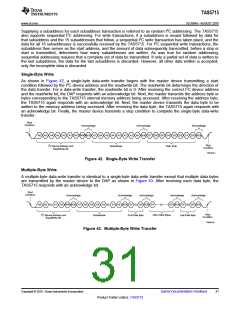
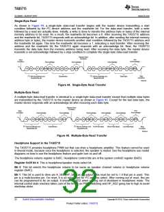
Single-Byte Read
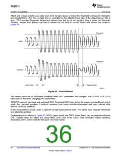
As shown in Figure 44, a single-byte data-read transfer begins with the master device transmitting a start
condition followed by the I2C device address and the read/write bit. For the data-read transfer, both a write
followed by a read are actually done. Initially, a write is done to transfer the address byte or bytes of the internal
memory address to be read. As a result, the read/write bit becomes a 0. After receiving the TAS5715 address
and the read/write bit, TAS5715 responds with an acknowledge bit. In addition, after sending the internal memory
address byte or bytes, the master device transmits another start condition followed by the TAS5715 address and
the read/write bit again. This time the read/write bit becomes a 1, indicating a read transfer. After receiving the
address and the read/write bit, the TAS5715 again responds with an acknowledge bit. Next, the TAS5715
transmits the data byte from the memory address being read. After receiving the data byte, the master device
transmits a not-acknowledge followed by a stop condition to complete the single-byte data-read transfer.
Repeat Start
Condition
Not
Acknowledge
Start
Condition
Acknowledge
Acknowledge
A0 ACK
Acknowledge
A6 A5
A1 A0 R/W ACK A7 A6 A5 A4
A6 A5
A1 A0 R/W ACK D7 D6
D1 D0 ACK
I2C Device Address and
Read/Write Bit
Subaddress
I2C Device Address and
Read/Write Bit
Data Byte
Stop
Condition
T0036-03
Figure 44. Single-Byte Read Transfer
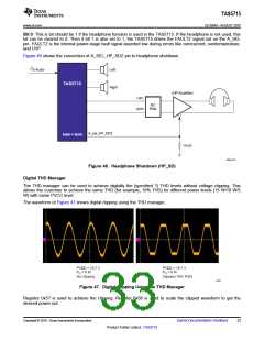
Multiple-Byte Read
A multiple-byte data-read transfer is identical to a single-byte data-read transfer except that multiple data bytes
are transmitted by the TAS5715 to the master device as shown in Figure 45. Except for the last data byte, the
master device responds with an acknowledge bit after receiving each data byte.
Repeat Start
Condition
Not
Acknowledge
Start
Condition
Acknowledge
Acknowledge
Acknowledge
Acknowledge
Acknowledge
D0 ACK D7
A6
A0 R/W ACK A7 A6 A5
A0 ACK
A6
A0 R/W ACK D7
D0 ACK D7
D0 ACK
I2C Device Address and
Read/Write Bit
Subaddress
I2C Device Address and First Data Byte
Read/Write Bit
Other Data Bytes
Last Data Byte
Stop
Condition
T0036-04
Figure 45. Multiple-Byte Read Transfer
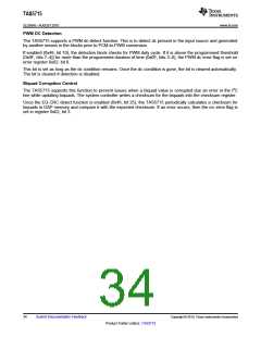
Headphone Support in the TAS5715
The TAS5715 provides headphone PWM out that can drive a headphone amplifier. This feature cannot be used
in lineout mode, because once the headphone is selected, the speaker is muted. See the headphone use model
diagrams on how to use the headphone feature and quite turn on and off.
The headphone volume register is 0x0C. Headphone control bits are in the system control2 register (0x05).
Register 0x05 bit 4: This is headphone/speaker mode-select bit.
Bit 3: This bit selects the headphone volume to be same as speaker channel volume or headphone volume
register (0x0C).
Bit 1: This bit is used to drive pin A_SEL_HP_SDZ as an output. This must be set to 1 if that pin is used. This
pin is a multi-function pin. On reset, it is an input used for I2C address select. After coming out of reset, this pin
can be programmed to be an output. It drives HP_SDZ when coming out of shutdown in headphone mode. The
internal control state machine takes care of the timing on PWM switching and HP_SDZ going low to high to avoid
start/stop clicks.
32
Submit Documentation Feedback
Copyright © 2010, Texas Instruments Incorporated
Product Folder Link(s): TAS5715

 TI [ TEXAS INSTRUMENTS ]