TAS5715
SLOS645 –AUGUST 2010
www.ti.com
PWM Section
The TAS5715 DAP device uses noise-shaping and sophisticated nonlinear correction algorithms to achieve high
power efficiency and high-performance digital audio reproduction. The DAP uses a fourth-order noise shaper to
increase dynamic range and SNR in the audio band. The PWM section accepts 24-bit PCM data from the DAP
and outputs two BTL PWM audio output channels.
The PWM section has individual-channel dc-blocking filters that can be enabled and disabled. The filter cutoff
frequency is less than 1 Hz. Individual-channel de-emphasis filters for 44.1- and 48-kHz are included and can be
enabled and disabled.
Finally, the PWM section has an adjustable maximum modulation limit of 93.8% to 99.2%.
For detailed description of using audio processing features like DRC, EQ, 3D, and bass boost, see the User's
Guide and TAS570X GDE software development tool documentation. Also see the GDE software development
tool for the device data path.
I2C COMPATIBLE SERIAL CONTROL INTERFACE
The TAS5715 DAP has an I2C serial control slave interface to receive commands from a system controller. The
serial control interface supports both normal-speed (100-kHz) and high-speed (400-kHz) operations without wait
states. As an added feature, this interface operates even if MCLK is absent.
The serial control interface supports both single-byte and multiple-byte read and write operations for status
registers and the general control registers associated with the PWM.
SERIAL INTERFACE CONTROL AND TIMING
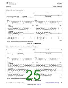
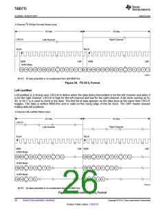
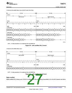
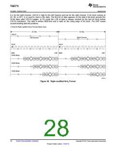
I2S Timing
I2S timing uses LRCLK to define when the data being transmitted is for the left channel and when it is for the
right channel. LRCLK is low for the left channel and high for the right channel. A bit clock running at 32, 48, or
64 × fS is used to clock in the data. There is a delay of one bit clock from the time the LRCLK signal changes
state to the first bit of data on the data lines. The data is written MSB-first and is valid on the rising edge of bit
clock. The DAP masks unused trailing data-bit positions.
24
Submit Documentation Feedback
Copyright © 2010, Texas Instruments Incorporated
Product Folder Link(s): TAS5715

 TI [ TEXAS INSTRUMENTS ]