TAS5727
SLOS670 –NOVEMBER 2010
www.ti.com
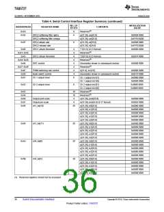
Table 4. Serial Control Interface Register Summary (continued)
NO. OF
BYTES
INITIALIZATION
SUBADDRESS
REGISTER NAME
CONTENTS
VALUE
0x3D
8
8
Reserved(3)
0x3E
DRC2 softening filter alpha
DRC2 softening filter omega
DRC2 attack rate
u[31:26], ae[25:0]
u[31:26], oe[25:0]
u[31:26], at[25:0]
u[31:26], rt[25:0]
0x0008 0000
0xFFF8 0000
0x0008 0000
0xFFF8 0000
0x0800 0000
0x3F
8
DRC2 release rate
0x40
0x41–0x42
0x43
DRC1 attack threshold
4
4
4
4
4
4
4
4
8
T1[31:0] (9.23 format)
Reserved(3)
DRC2 attack threshold
DRC control
T2[31:0] (9.23 format)
Reserved(3)
0x0074 0000
0x0000 0000
0x44–0x45
0x46
Description shown in subsequent section
Reserved(3)
0x47–0x4E
0x4F
PWM switching rate control
Bank switch control
u[31:4], src[3:0]
0x0000 0006
0x0F70 8000
0x0080 0000
0x0000 0000
0x0080 0000
0x0000 0000
0x50
Description shown in subsequent section
Ch 1 output mix1[1]
Ch 1 output mix1[0]
Ch 2 output mix2[1]
Ch 2 output mix2[0]
Reserved(3)
0x51
Ch 1 output mixer
0x52
Ch 2 output mixer
8
0x53
0x54
0x56
0x57
0x58
16
16
4
Reserved(3)
Output post-scale
Output pre-scale
ch1_bq[10]
u[31:26], post[25:0]
u[31:26], pre[25:0] (9.17 format)
u[31:26], b0[25:0]
u[31:26], b1[25:0]
u[31:26], b2[25:0]
u[31:26], a1[25:0]
u[31:26], a2[25:0]
u[31:26], b0[25:0]
u[31:26], b1[25:0]
u[31:26], b2[25:0]
u[31:26], a1[25:0]
u[31:26], a2[25:0]
u[31:26], b0[25:0]
u[31:26], b1[25:0]
u[31:26], b2[25:0]
u[31:26], a1[25:0]
u[31:26], a2[25:0]
u[31:26], b0[25:0]
u[31:26], b1[25:0]
u[31:26], b2[25:0]
u[31:26], a1[25:0]
u[31:26], a2[25:0]
0x0080 0000
0x0002 0000
0x0080 0000
0x0000 0000
0x0000 0000
0x0000 0000
0x0000 0000
0x0080 0000
0x0000 0000
0x0000 0000
0x0000 0000
0x0000 0000
0x0080 0000
0x0000 0000
0x0000 0000
0x0000 0000
0x0000 0000
0x0080 0000
0x0000 0000
0x0000 0000
0x0000 0000
0x0000 0000
4
20
0x59
0x5A
0x5B
ch1_bq[11]
ch4_bq[0]
ch4_bq[1]
20
20
20
(3) Reserved registers should not be accessed.
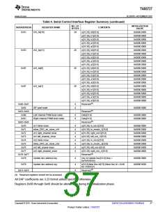
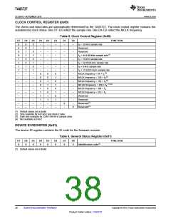
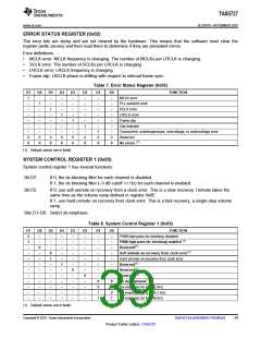
36
Submit Documentation Feedback
Copyright © 2010, Texas Instruments Incorporated
Product Folder Link(s): TAS5727

 TI [ TEXAS INSTRUMENTS ]