2G80
DUAL POSITIVE-EDGE-TRIGGERED D-TYPE FLIP-FLOP
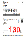
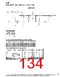
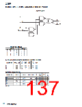
Logic Diagram
C
CLK
C
C
TG
Q
C
C
C
C
D
TG
TG
TG
C
C
C
FUNCTION TABLE
(each flip-flop)
INPUTS
OUTPUT
Q
CLK
D
H
L
↑
↑
L
L
H
X
Q
0
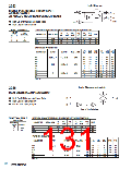
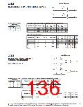
ELECTRICAL CHARACTERISTICS AND RECOMMENDED OPERATING CONDITIONS
LVC
5V
LVC
3.3V
LVC
2.5V
LVC
1.8V
AUC
AUC
PARAMETER
MAX or MIN
UNIT
2.5V 1.8V
ICC
IOH
IOL
MAX
MAX
MAX
0.005 0.005 0.005 0.005
0.01
-9
9
0.01
-8
8
mA
mA
mA
-32
32
-24
24
-8
8
-4
4
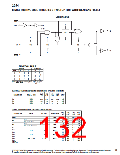
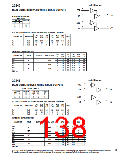
TIMING REQUREMENTS AND SWITCHING CHARACTERISTICS
LVC
5V
LVC
3.3V
LVC
2.5V
LVC
1.8V
AUC
AUC
PARAMETER
INPUT
OUTPUT
MAX or MIN
2.5V 1.8V
fmax
tw
MIN
MIN
160
2.5
0.9
0.9
0.6
4.5
4.5
160
2.5
1.1
1.1
0.8
5.2
5.2
160
2.5
1.4
1.4
1.0
7.0
7.0
160
2.5
2.2
2.2
1.6
275
1
250
1
CLK high or low
Before CLK ↑ , Data high
Before CLK ↑ , Data low
Data after CLK ↑
0.5
0.5
0.5
1.8
1.8
0.6
0.6
0.1
2.4
2.4
tsu
MIN
th
tPLH
tPHL
MIN
13.9
13.9
CLK
Q
MAX
UNIT fmax : MHz other : ns
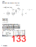
129
PRODUCTION DATA information is current as of publication date. Products conform to specifications per the terms of Texas Instruments standard warranty.
Production processing does not necessarily include testing of all parameters. See www.ti.com/sc/logic for the most current data sheets.

 TI [ TEXAS INSTRUMENTS ]