SN74LVC1G3157
SINGLE-POLE, DOUBLE-THROW ANALOG SWITCH
SCES424C – JANUARY 2003 - REVISED SEPTEMBER 2003
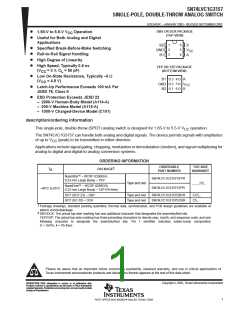
FUNCTION TABLE
CONTROL
ON
INPUT
S
CHANNEL
L
B1
B2
H
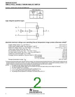
logic diagram (positive logic)
1
B2
6
4
A
S
3
B1
†
absolute maximum ratings over operating free-air temperature range (unless otherwise noted)
Supply voltage range, V
(see Note 1) . . . . . . . . . . . . . . . . . . . . . . . . . . . . . . . . . . . . . . . . . . . . . –0.5 V to 6.5 V
CC
Control input voltage range, V (see Notes 1 and 2) . . . . . . . . . . . . . . . . . . . . . . . . . . . . . . . . . . –0.5 V to 6.5 V
Switch I/O voltage range, V (see Notes 1, 2, 3, and 4) . . . . . . . . . . . . . . . . . . . . . . . . . –0.5 V to V
Control input clamp current, I (V < 0) . . . . . . . . . . . . . . . . . . . . . . . . . . . . . . . . . . . . . . . . . . . . . . . . . . . –50 mA
IN
I/O
+ 0.5 V
CC
IK IN
I/O port diode current, I
(V < 0 or V > V ) . . . . . . . . . . . . . . . . . . . . . . . . . . . . . . . . . . . . . . . . . 50 mA
IOK I/O
I/O CC
On-state switch current, I (V = 0 to V ) (see Note 5) . . . . . . . . . . . . . . . . . . . . . . . . . . . . . . . . . . 128 mA
Continuous current through V
I/O I/O
CC
or GND . . . . . . . . . . . . . . . . . . . . . . . . . . . . . . . . . . . . . . . . . . . . . . . . . . 100 mA
CC
Package thermal impedance, θ (see Note 6): DBV package . . . . . . . . . . . . . . . . . . . . . . . . . . . . . . . 165°C/W
JA
DCK package . . . . . . . . . . . . . . . . . . . . . . . . . . . . . . . 259°C/W
YEP/YZP package . . . . . . . . . . . . . . . . . . . . . . . . . . . 123°C/W
. . . . . . . . . . . . . . . . . . . . . . . . . . . . . . . . . . . . . . . . . . . . . . . . . . . –65°C to 150°C
Storage temperature range, T
stg
†
Stresses beyond those listed under “absolute maximum ratings” may cause permanent damage to the device. These are stress ratings only, and
functional operation of the device at these or any other conditions beyond those indicated under “recommended operating conditions” is not
implied. Exposure to absolute-maximum-rated conditions for extended periods may affect device reliability.
NOTES: 1. All voltages are with respect to ground unless otherwise specified.
2. The input and output voltage ratings may be exceeded if the input and output clamp-current ratings are observed.
3. This value is limited to 5.5 V maximum.
4. V , V , V , and V are used to denote specific conditions for V
Bn I/O
.
I
O
A
5. I , I , I , and I are used to denote specific conditions for I .
I
O
A
Bn
I/O
6. The package thermal impedance is calculated in accordance with JESD 51-7.
2
POST OFFICE BOX 655303 • DALLAS, TEXAS 75265

 TI [ TEXAS INSTRUMENTS ]