SN74LVC1T45-Q1
SCES677A –SEPTEMBER 2006–REVISED AUGUST 2009 .......................................................................................................................................... www.ti.com
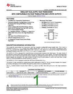
FUNCTION TABLE(1)
INPUT
OPERATION
DIR
L
B data to A bus
A data to B bus
H
(1) Input circuits of the data I/Os
always are active.
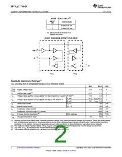
LOGIC DIAGRAM (POSITIVE LOGIC)
5
3
DIR
A
4
B
VCCA
VCCB
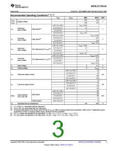
Absolute Maximum Ratings(1)
over operating free-air temperature range (unless otherwise noted)
MIN
MAX
UNIT
VCCA
Supply voltage range
VCCB
–0.5
6.5
V
VI
Input voltage range(2)
Voltage range applied to any output in the high-impedance or power-off state(2)
–0.5
–0.5
6.5
6.5
V
V
VO
A port
Voltage range applied to any output in the high or low state(2) (3)
B port
–0.5 VCCA + 0.5
VO
V
–0.5 VCCB + 0.5
IIK
IOK
IO
Input clamp current
VI < 0
–50
–50
mA
mA
mA
mA
°C/W
°C
Output clamp current
VO < 0
Continuous output current
Continuous current through VCC or GND
Package thermal impedance(4)
Storage temperature range
±50
±100
259
θJA
DCK package
Tstg
–65
150
(1) Stresses beyond those listed under "absolute maximum ratings" may cause permanent damage to the device. These are stress ratings
only, and functional operation of the device at these or any other conditions beyond those indicated under "recommended operating
conditions" is not implied. Exposure to absolute-maximum-rated conditions for extended periods may affect device reliability.
(2) The input and output negative-voltage ratings may be exceeded if the input and output clamp-current ratings are observed.
(3) The value of VCC is provided in the recommended operating conditions table.
(4) The package thermal impedance is calculated in accordance with JESD 51-7.
2
Submit Documentation Feedback
Copyright © 2006–2009, Texas Instruments Incorporated
Product Folder Link(s): SN74LVC1T45-Q1

 TI [ TEXAS INSTRUMENTS ]