SN74LVC1T45-Q1
www.ti.com .......................................................................................................................................... SCES677A –SEPTEMBER 2006–REVISED AUGUST 2009
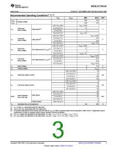
Operating Characteristics
TA = 25°C
VCCA
VCCB = 1.8 V
=
VCCA
VCCB = 2.5 V
=
VCCA
VCCB = 3.3 V
=
VCCA =
VCCB = 5 V
TEST
CONDITIONS
PARAMETER
UNIT
TYP
TYP
TYP
TYP
A-port input,
B-port output
3
18
18
3
4
19
19
4
4
20
20
4
4
21
21
4
CL = 0 pF,
f = 10 MHz,
tr = tf = 1 ns
(1)
CpdA
pF
B-port input,
A-port output
A-port input,
B-port output
CL = 0 pF,
f = 10 MHz,
tr = tf = 1 ns
(1)
CpdB
pF
B-port input,
A-port output
(1) Power dissipation capacitance per transceiver
Power-Up Considerations
A proper power-up sequence always should be followed to avoid excessive supply current, bus contention,
oscillations, or other anomalies. To guard against such power-up problems, take the following precautions:
1. Connect ground before any supply voltage is applied.
2. Power up VCCA
.
3. VCCB can be ramped up along with or after VCCA
.
Copyright © 2006–2009, Texas Instruments Incorporated
Submit Documentation Feedback
7
Product Folder Link(s): SN74LVC1T45-Q1

 TI [ TEXAS INSTRUMENTS ]