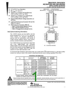
ꢀꢁ ꢂꢃ ꢄꢅꢆ ꢇ ꢈ ꢉꢊ ꢀꢁ ꢈꢃ ꢄꢅ ꢆꢇ ꢈꢉ
ꢋꢌ ꢍ ꢎꢏꢐ ꢐ ꢌꢑꢀ ꢉꢁꢒ ꢄ ꢓꢁꢌ ꢒ ꢑꢓ ꢅ ꢌꢑ ꢀ
ꢔ ꢓꢕ ꢋ ꢆ ꢖꢀꢕꢉꢕ ꢌ ꢗ ꢏꢕ ꢘ ꢏꢕꢀ
SCLS398G − APRIL 1998 − REVISED APRIL 2005
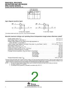
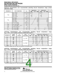
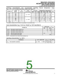
switching characteristics over recommended operating free-air temperature range,
V
= 5 V 0.5 V (unless otherwise noted) (see Figure 1)
CC
T
A
= 25°C
TYP
3.6*
SN54LV367A SN74LV367A
FROM
(INPUT)
TO
(OUTPUT)
LOAD
CAPACITANCE
PARAMETER
UNIT
MIN
MAX
5.9*
7.2*
7.2*
MIN
1*
MAX
7*
MIN
1
MAX
7
t
t
t
t
t
t
A
Y
Y
Y
Y
Y
Y
pd
en
dis
pd
en
dis
3.8*
1*
8.5*
8.5*
1
8.5
8.5
OE
OE
A
C
C
= 15 pF
= 50 pF
ns
L
L
2.6*
1*
0
4.5
4.9
4.5
7.9
9.2
9.2
1
1
1
9
10.5
10.5
1
1
0
9
10.5
10.5
OE
OE
ns
t
1
1
sk(o)
* On products compliant to MIL-PRF-38535, this parameter is not production tested.
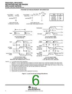
noise characteristics, V
= 3.3 V, C = 50 pF, T = 25°C (see Note 5)
CC
L
A
SN74LV367A
PARAMETER
UNIT
MIN
TYP
0.5
−0.2
3
MAX
V
V
V
V
V
Quiet output, maximum dynamic V
0.8
V
V
V
V
V
OL(P)
OL(V)
OH(V)
IH(D)
IL(D)
OL
Quiet output, minimum dynamic V
Quiet output, minimum dynamic V
High-level dynamic input voltage
Low-level dynamic input voltage
−0.8
OL
OH
2.31
0.99
NOTE 5: Characteristics are for surface-mount packages only.
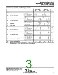
operating characteristics, T = 25°C
A
PARAMETER
TEST CONDITIONS
= 50 pF, f = 10 MHz
L
V
TYP
14.9
17.4
UNIT
CC
3.3 V
C
Power dissipation capacitance
C
pF
pd
5 V
ꢘ
ꢑ
ꢗ
ꢒ
ꢏ
ꢥ
ꢕ
ꢘ
ꢑ
ꢌ
ꢅ
ꢓ
ꢌ
ꢔ
ꢛ
ꢣ
ꢦ
ꢞ
ꢧ
ꢡ
ꢤ
ꢙ
ꢛ
ꢞ
ꢣ
ꢟ
ꢞ
ꢣ
ꢟ
ꢢ
ꢧ
ꢣ
ꢜ
ꢨ
ꢧ
ꢞ
ꢝ
ꢠ
ꢝꢢ ꢜ ꢛ ꢯꢣ ꢨꢚ ꢤ ꢜ ꢢ ꢞꢦ ꢝꢢ ꢰ ꢢ ꢪꢞ ꢨꢡꢢ ꢣꢙꢫ ꢥ ꢚꢤ ꢧꢤ ꢟꢙ ꢢꢧ ꢛꢜ ꢙꢛ ꢟ ꢝꢤ ꢙꢤ ꢤꢣ ꢝ ꢞꢙ ꢚꢢꢧ
ꢟ
ꢙ
ꢜ
ꢛ
ꢣ
ꢙ
ꢚ
ꢢ
ꢦ
ꢞ
ꢧ
ꢡ
ꢤ
ꢙ
ꢛ
ꢰ
ꢢ
ꢞ
ꢧ
ꢜ
ꢨ
ꢢ
ꢟ
ꢛ
ꢦ
ꢛ
ꢟ
ꢤ
ꢙ
ꢛ
ꢞ
ꢣ
ꢜ
ꢤ
ꢧ
ꢢ
ꢝ
ꢢ
ꢜ
ꢛ
ꢯ
ꢣ
ꢯ
ꢞ
ꢤ
ꢪ
ꢜ
ꢫ
ꢕ
ꢢ
ꢬ
ꢤ
ꢜ
ꢓ
ꢣ
ꢜ
ꢙ
ꢧ
ꢠ
ꢡ
ꢢ
ꢣ
ꢟ ꢚꢤ ꢣ ꢯꢢ ꢞꢧ ꢝꢛ ꢜ ꢟ ꢞꢣ ꢙꢛ ꢣꢠꢢ ꢙ ꢚꢢ ꢜ ꢢ ꢨꢧ ꢞꢝ ꢠꢟꢙ ꢜ ꢭ ꢛꢙꢚ ꢞꢠꢙ ꢣꢞꢙ ꢛꢟꢢ ꢫ
ꢙ
ꢜ
ꢧ
ꢢ
ꢜ
ꢢ
ꢧ
ꢰ
ꢢ
ꢜ
ꢙ
ꢚ
ꢢ
ꢧ
ꢛ
ꢯ
ꢚ
ꢙ
ꢙ
ꢞ
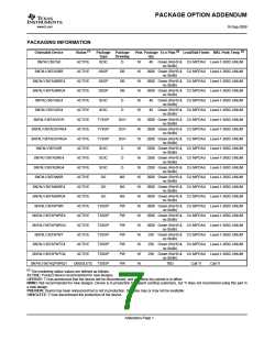
5
POST OFFICE BOX 655303 • DALLAS, TEXAS 75265

 TI [ TEXAS INSTRUMENTS ]