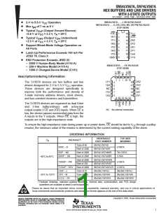
ꢀ ꢁꢂ ꢃꢄꢅꢆ ꢇ ꢈꢉ ꢊ ꢀꢁ ꢈꢃ ꢄꢅ ꢆ ꢇꢈ ꢉ
ꢋ ꢌꢍ ꢎ ꢏꢐ ꢐ ꢌ ꢑꢀ ꢉꢁ ꢒ ꢄꢓ ꢁ ꢌ ꢒꢑ ꢓ ꢅꢌ ꢑꢀ
ꢔꢓ ꢕ ꢋ ꢆ ꢖꢀꢕꢉꢕ ꢌ ꢗꢏꢕ ꢘ ꢏꢕꢀ
SCLS398G − APRIL 1998 − REVISED APRIL 2005
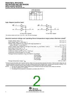
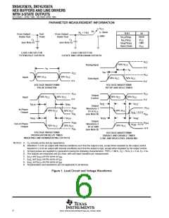
FUNCTION TABLE
(each buffer/driver)
INPUTS
OUTPUT
Y
OE
A
H
L
L
L
H
L
H
X
Z
logic diagram (positive logic)
1
15
1OE
2OE
2A1
2
3
12
11
1A1
1Y1
2Y1
To Three Other Channels
Pin numbers shown are for the D, DB, DGV, J, NS, PW, and W packages.
To One Other Channel
†
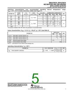
absolute maximum ratings over operating free-air temperature range (unless otherwise noted)
Supply voltage range, V
. . . . . . . . . . . . . . . . . . . . . . . . . . . . . . . . . . . . . . . . . . . . . . . . . . . . . . . . . . −0.5 V to 7 V
CC
Input voltage range, V (see Note 1) . . . . . . . . . . . . . . . . . . . . . . . . . . . . . . . . . . . . . . . . . . . . . . . . . . −0.5 V to 7 V
I
Voltage range applied to any output in the high-impedance or
power-off state, V (see Note 1) . . . . . . . . . . . . . . . . . . . . . . . . . . . . . . . . . . . . . . . . . . . . . . . . . . . −0.5 V to 7 V
O
Output voltage range applied in the high or low state, V (see Notes 1 and 2) . . . . . . −0.5 V to V
+ 0.5 V
O
CC
Input clamp current, I (V < 0) . . . . . . . . . . . . . . . . . . . . . . . . . . . . . . . . . . . . . . . . . . . . . . . . . . . . . . . . . . . −20 mA
IK
I
Output clamp current, I
(V < 0) . . . . . . . . . . . . . . . . . . . . . . . . . . . . . . . . . . . . . . . . . . . . . . . . . . . . . . . . −50 mA
OK
O
Continuous output current, I (V = 0 to V ) . . . . . . . . . . . . . . . . . . . . . . . . . . . . . . . . . . . . . . . . . . . . . . 35 mA
Continuous current through V
O
O
CC
CC
or GND . . . . . . . . . . . . . . . . . . . . . . . . . . . . . . . . . . . . . . . . . . . . . . . . . . . 70 mA
Package thermal impedance, θ (see Note 3): D package . . . . . . . . . . . . . . . . . . . . . . . . . . . . . . . . . . . 73°C/W
JA
DB package . . . . . . . . . . . . . . . . . . . . . . . . . . . . . . . . . 82°C/W
DGV package . . . . . . . . . . . . . . . . . . . . . . . . . . . . . . . 120°C/W
NS package . . . . . . . . . . . . . . . . . . . . . . . . . . . . . . . . . 64°C/W
PW package . . . . . . . . . . . . . . . . . . . . . . . . . . . . . . . . 108°C/W
Storage temperature range, T
. . . . . . . . . . . . . . . . . . . . . . . . . . . . . . . . . . . . . . . . . . . . . . . . . . . −65°C to 150°C
stg
†
Stresses beyond those listed under “absolute maximum ratings” may cause permanent damage to the device. These are stress ratings only, and
functional operation of the device at these or any other conditions beyond those indicated under “recommended operating conditions” is not
implied. Exposure to absolute-maximum-rated conditions for extended periods may affect device reliability.
NOTES: 1. The input and output negative-voltage ratings may be exceeded if the input and output current ratings are observed.
2. This value is limited to 5.5 V maximum.
3. The package thermal impedance is calculated in accordance with JESD 51-7.
2
POST OFFICE BOX 655303 • DALLAS, TEXAS 75265

 TI [ TEXAS INSTRUMENTS ]