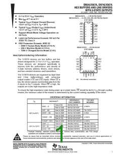
ꢀꢁ ꢂꢃ ꢄꢅꢆ ꢇ ꢈ ꢉꢊ ꢀꢁ ꢈꢃ ꢄꢅ ꢆꢇ ꢈꢉ
ꢋꢌ ꢍ ꢎꢏꢐ ꢐ ꢌꢑꢀ ꢉꢁꢒ ꢄ ꢓꢁꢌ ꢒ ꢑꢓ ꢅ ꢌꢑ ꢀ
ꢔ ꢓꢕ ꢋ ꢆ ꢖꢀꢕꢉꢕ ꢌ ꢗ ꢏꢕ ꢘ ꢏꢕꢀ
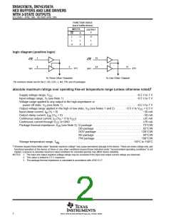
SCLS398G − APRIL 1998 − REVISED APRIL 2005
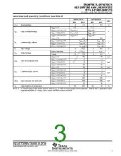
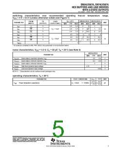
recommended operating conditions (see Note 4)
SN54LV367A
SN74LV367A
UNIT
MIN
2
MAX
MIN
2
MAX
V
V
Supply voltage
5.5
5.5
V
CC
V
V
V
V
V
V
V
V
= 2 V
1.5
1.5
CC
CC
CC
CC
CC
CC
CC
CC
= 2.3 V to 2.7 V
= 3 V to 3.6 V
= 4.5 V to 5.5 V
= 2 V
V
V
V
× 0.7
V
V
V
× 0.7
CC
CC
CC
CC
CC
CC
High-level input voltage
V
IH
× 0.7
× 0.7
× 0.7
× 0.7
0.5
0.5
= 2.3 V to 2.7 V
= 3 V to 3.6 V
= 4.5 V to 5.5 V
V
V
V
× 0.3
× 0.3
× 0.3
V
V
V
× 0.3
× 0.3
× 0.3
CC
CC
CC
CC
CC
CC
V
IL
Low-level input voltage
V
V
V
V
Input voltage
0
0
0
5.5
0
0
0
5.5
I
High or low state
3-state
V
V
CC
5.5
CC
5.5
Output voltage
V
O
V
CC
V
CC
V
CC
V
CC
V
CC
V
CC
V
CC
V
CC
V
CC
V
CC
V
CC
= 2 V
−50
−2
−50
−2
−8
−16
50
2
µA
= 2.3 V to 2.7 V
= 3 V to 3.6 V
= 4.5 V to 5.5 V
= 2 V
I
High-level output current
Low-level output current
OH
OL
−8
mA
−16
50
µA
= 2.3 V to 2.7 V
= 3 V to 3.6 V
= 4.5 V to 5.5 V
= 2.3 V to 2.7 V
= 3 V to 3.6 V
= 4.5 V to 5.5 V
2
I
8
8
mA
16
16
200
100
20
85
200
100
20
∆t/∆v
Input transition rise or fall rate
Operating free-air temperature
ns/V
T
−55
125
−40
°C
A
NOTE 4: All unused inputs of the device must be held at V
or GND to ensure proper device operation. Refer to the TI application report,
Implications of Slow or Floating CMOS Inputs, literature number SCBA004.
CC
ꢘ
ꢑ
ꢗ
ꢒ
ꢏ
ꢥ
ꢕ
ꢘ
ꢑ
ꢌ
ꢅ
ꢓ
ꢌ
ꢔ
ꢛ
ꢣ
ꢦ
ꢞ
ꢧ
ꢡ
ꢤ
ꢙ
ꢛ
ꢞ
ꢣ
ꢟ
ꢞ
ꢣ
ꢟ
ꢢ
ꢧ
ꢣ
ꢜ
ꢨ
ꢧ
ꢞ
ꢝ
ꢠ
ꢝꢢ ꢜ ꢛ ꢯꢣ ꢨꢚ ꢤ ꢜ ꢢ ꢞꢦ ꢝꢢ ꢰ ꢢ ꢪꢞ ꢨꢡꢢ ꢣꢙꢫ ꢥ ꢚꢤ ꢧꢤ ꢟꢙ ꢢꢧ ꢛꢜ ꢙꢛ ꢟ ꢝꢤ ꢙꢤ ꢤꢣ ꢝ ꢞꢙ ꢚꢢꢧ
ꢟ
ꢙ
ꢜ
ꢛ
ꢣ
ꢙ
ꢚ
ꢢ
ꢦ
ꢞ
ꢧ
ꢡ
ꢤ
ꢙ
ꢛ
ꢰ
ꢢ
ꢞ
ꢧ
ꢜ
ꢨ
ꢢ
ꢟ
ꢛ
ꢦ
ꢛ
ꢟ
ꢤ
ꢙ
ꢛ
ꢞ
ꢣ
ꢜ
ꢤ
ꢧ
ꢢ
ꢝ
ꢢ
ꢜ
ꢛ
ꢯ
ꢣ
ꢯ
ꢞ
ꢤ
ꢪ
ꢜ
ꢫ
ꢕ
ꢢ
ꢬ
ꢤ
ꢜ
ꢓ
ꢣ
ꢜ
ꢙ
ꢧ
ꢠ
ꢡ
ꢢ
ꢣ
ꢟ ꢚꢤ ꢣ ꢯꢢ ꢞꢧ ꢝꢛ ꢜ ꢟ ꢞꢣ ꢙꢛ ꢣꢠꢢ ꢙ ꢚꢢ ꢜ ꢢ ꢨꢧ ꢞꢝ ꢠꢟꢙ ꢜ ꢭ ꢛꢙꢚ ꢞꢠꢙ ꢣꢞꢙ ꢛꢟꢢ ꢫ
ꢙ
ꢜ
ꢧ
ꢢ
ꢜ
ꢢ
ꢧ
ꢰ
ꢢ
ꢜ
ꢙ
ꢚ
ꢢ
ꢧ
ꢛ
ꢯ
ꢚ
ꢙ
ꢙ
ꢞ
3
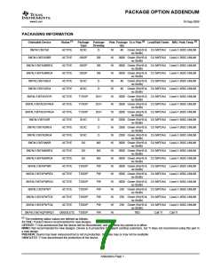
POST OFFICE BOX 655303 • DALLAS, TEXAS 75265

 TI [ TEXAS INSTRUMENTS ]