SN65HVD230
SN65HVD231
SN65HVD232
SLOS346G – MARCH 2001 – REVISED JUNE 2002
device switching characteristics over recommended operating conditions (unless otherwise
noted)
TEST
CONDITIONS
PARAMETER
MIN
TYP
MAX
UNIT
V
= 0 V,
See Figure 9
See Figure 9
70
105
535
100
155
830
115
175
920
135
185
990
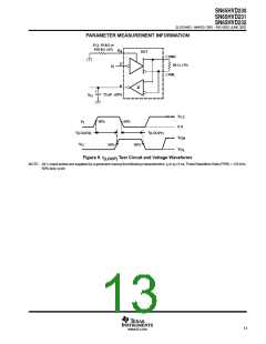
(Rs)
Total loop delay, driver input to receiver
output, recessive to dominant
R
R
with 10 kΩ to ground,
t
t
ns
S
(LOOP1)
with 100 kΩ to ground, See Figure 9
S
V
(Rs)
= 0 V,
See Figure 9
See Figure 9
Total loop delay, driver input to receiver
output, dominant to recessive
R
R
with 10 kΩ to ground,
ns
S
S
(LOOP2)
with 100 kΩ to ground, See Figure 9
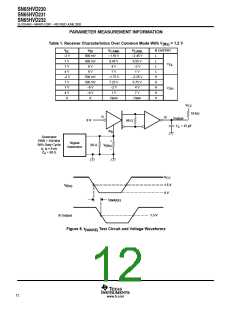
device control-pin characteristics over recommended operating conditions (unless otherwise
noted)
†
PARAMETER
TEST CONDITIONS
MIN
TYP
MAX
1.5
5
UNIT
µS
SN65HVD230 wake-up time from standby mode with R
0.55
3
S
t
See Figure 8
(WAKE)
SN65HVD231 wake-up time from sleep mode with R
µS
S
–5 µA < I
< 5 µA
0.45 V
0.55 V
(Vref)
–50 µA < I
CC
CC
V
Reference output voltage
Input current for high-speed
V
ref
< 50 µA
0.4 V
0.6 V
(Vref)
< 1 V
(Rs)
CC
CC
I
V
–450
0
µA
(Rs)
†
All typical values are at 25°C and with a 3.3-V supply.
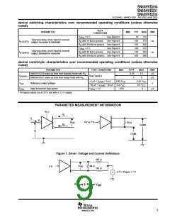
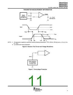
PARAMETER MEASUREMENT INFORMATION
V
CC
I
O
O
I
I
D
0 V or 3 V
V
OD
60 Ω
I
CANH
V
I
CANL
Figure 1. Driver Voltage and Current Definitions
167 Ω
V
OD
60 Ω
0 V
167 Ω
–2 V ≤ V
TEST
≤ 7 V
±
Figure 2. Driver V
OD
9
www.ti.com

 TI [ TEXAS INSTRUMENTS ]