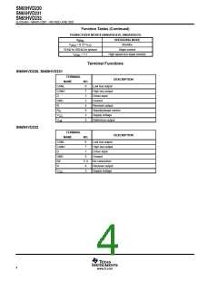
SN65HVD230
SN65HVD231
SN65HVD232
SLOS346G – MARCH 2001 – REVISED JUNE 2002
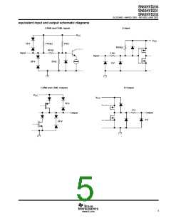
driver switching characteristics over recommended operating conditions(unless otherwise noted)
SN65HVD232
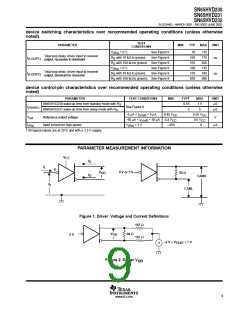
PARAMETER
TEST CONDITIONS
MIN
TYP
35
MAX
85
UNIT
ns
t
t
t
t
t
Propagation delay time, low-to-high-level output
Propagation delay time, high-to-low-level output
PLH
PHL
sk(p)
r
70
120
ns
Pulse skew (|t
– t
P(HL) P(LH)
|)
35
ns
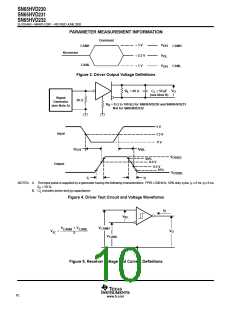
C
= 50 pF, See Figure 4
L
Differential output signal rise time
Differential output signal fall time
25
40
50
100
80
ns
55
ns
f
receiver electrical characteristics over recommended operating conditions (unless otherwise
noted)
†
PARAMETER
TEST CONDITIONS
MIN TYP
MAX
UNIT
V
V
V
V
V
Positive-going input threshold voltage
Negative-going input threshold voltage
750
650
100
900
mV
IT+
IT–
hys
OH
OL
See Table 1
500
2.4
mV
V
Hysteresis voltage (V )
V
IT+ – IT–
High-level output voltage
Low-level output voltage
–6 V ≤ V ≤ 500 mV, I = –8 mA, See Figure 5
ID
O
900 mV ≤ V ≤ 6 V, I = 8 mA, See Figure 5
0.4
250
350
–30
–20
ID
O
V
IH
V
IH
V
IH
V
IH
= 7 V
100
100
µA
= 7 V,
= –2 V
V
= 0 V
CC
CC
Other input at 0 V,
D = 3 V
I
I
Bus input current
–200
–100
µA
pF
pF
= –2 V, V
= 0 V
Pin-to-ground,
V = 0.4 sin(4E6πt) + 0.5 V
I
V
V
= 3 V,
= 3 V,
(D)
C
C
CANH, CANL input capacitance
32
16
i
Pin-to-pin,
V = 0.4 sin(4E6πt) + 0.5 V
I
(D)
Differential input capacitance
Differential input resistance
diff
R
R
Pin-to-pin,
V
= 3 V
(D)
40
20
70
35
100
50
kΩ
kΩ
diff
I
CANH, CANL input resistance
Supply current
I
See driver
CC
†
All typical values are at 25°C and with a 3.3-V supply.
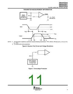
receiver switching characteristics over recommended operating conditions (unless otherwise
noted)
TEST
CONDITIONS
PARAMETER
MIN
TYP
MAX
UNIT
t
t
t
t
t
Propagation delay time, low-to-high-level output
Propagation delay time, high-to-low-level output
35
35
50
50
10
ns
ns
ns
ns
ns
PLH
PHL
sk(p)
r
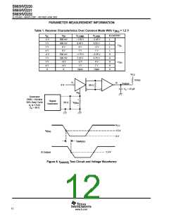
See Figure 6
Pulse skew (|t
– t |)
P(HL) P(LH)
Output signal rise time
Output signal fall time
1.5
1.5
See Figure 6
f
8
www.ti.com

 TI [ TEXAS INSTRUMENTS ]