SN65HVD230
SN65HVD231
SN65HVD232
SLOS346G – MARCH 2001 – REVISED JUNE 2002
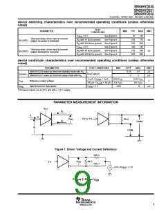
PARAMETER MEASUREMENT INFORMATION
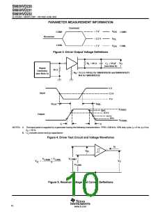
Dominant
≈ 3 V
V
OH
V
OL
V
OH
CANH
CANH
CANL
Recessive
≈ 2.3 V
≈ 1 V
CANL
Figure 3. Driver Output Voltage Definitions
V
O
R
= 60 Ω
C = 50 pF
L
(see Note B)
L
Signal
Generator
(see Note A)
50 Ω
R
= 0 Ω to 100 kΩ for SN65HVD230 and SN65HVD231
N/A for SN65HVD232
S
3 V
Input
1.5 V
0 V
t
t
PHL
PLH
V
OD(D)
90%
0.9 V
Output
0.5 V
10%
V
OD(R)
t
t
f
r
NOTES: A. The input pulse is supplied by a generator having the following characteristics: PRR ≤ 500 kHz, 50% duty cycle, t ≤ 6 ns, t ≤ 6 ns,
r
f
Z
C
= 50 Ω.
o
L
B.
includes probe and jig capacitance.
Figure 4. Driver Test Circuit and Voltage Waveforms
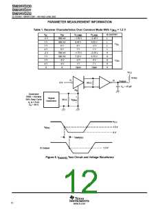
I
O
V
ID
V
) V
V
CANH
CANH
CANL
V
+
V
O
IC
2
V
CANL
Figure 5. Receiver Voltage and Current Definitions
10
www.ti.com

 TI [ TEXAS INSTRUMENTS ]