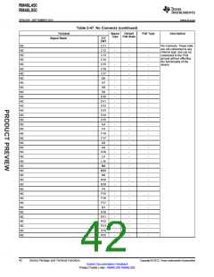
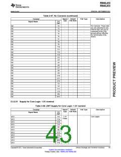
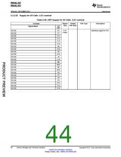
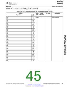
RM46L450
RM46L850
SPNS184 –SEPTEMBER 2012
www.ti.com
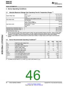
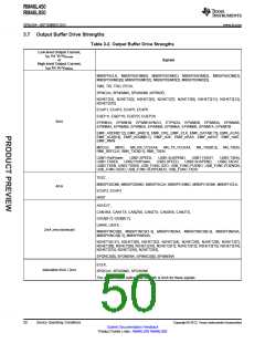
3 Device Operating Conditions
(1)
3.1 Absolute Maximum Ratings Over Operating Free-Air Temperature Range,
(2)
VCC
-0.3 V to 1.43 V
-0.3 V to 4.1 V
-0.3 V to 5.5 V
-0.3 V to 4.1 V
-0.3 V to 5.25 V
±20 mA
(2)
Supply voltage range:
Input voltage range:
VCCIO, VCCP
VCCAD
All input pins, with exception of ADC pins
ADC input pins
IIK (VI < 0 or VI > VCCIO
)
All pins, except AD1IN[23:0]
Input clamp current:
IIK (VI < 0 or VI > VCCAD
AD1IN[23:0]
)
±10 mA
Total
±40 mA
-40°C to 105°C
-40°C to 150°C
-65°C to 150°C
Operating free-air temperature range, TA:
Operating junction temperature range, TJ:
Storage temperature range, Tstg
(1) Stresses beyond those listed under “absolute maximum ratings” may cause permanent damage to the device. These are stress ratings
only, and functional operation of the device at these or any other conditions beyond those indicated under “recommended operating
conditions” is not implied. Exposure to absolute-maximum-rated conditions for extended periods may affect device reliability.
(2) maximum-rated conditions for extended periods may affect device reliability. All voltage values are with respect to their associated
grounds.
3.2 Device Recommended Operating Conditions(1)
MIN
1.14
1.14
3
NOM
1.2
MAX UNIT
VCC
Digital logic supply voltage (Core)
PLL Supply Voltage
1.32
1.32
3.6
V
V
VCCPLL
VCCIO
VCCAD
VCCP
VSS
1.2
Digital logic supply voltage (I/O)
MibADC supply voltage
3.3
V
3
5.25
3.6
V
Flash pump supply voltage
Digital logic supply ground
3
3.3
0
V
V
VSSAD
VADREFHI
VADREFLO
TA
MibADC supply ground
-0.1
VSSAD
VSSAD
-40
0.1
VCCAD
VCCAD
105
V
A-to-D high-voltage reference source
A-to-D low-voltage reference source
Operating free-air temperature
Operating junction temperature
V
V
°C
°C
TJ
-40
150
(1) All voltages are with respect to VSS, except VCCAD, which is with respect to VSSAD
46
Device Operating Conditions
Copyright © 2012, Texas Instruments Incorporated
Submit Documentation Feedback
Product Folder Links: RM46L450 RM46L850

 TI [ TEXAS INSTRUMENTS ]