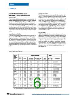
Application Notes
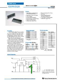
PT6940 Series
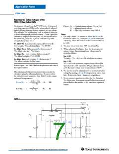
Adjusting the Output Voltages of the
PT6940 Dual-Output ISRs
Each output voltage from the PT6940 series of integrated
switching regulators (ISRs) can be independently adjusted
higher or lower than the factory trimmed pre-set voltage.
The voltages, Vo1 and Vo2 may each be adjusted either up
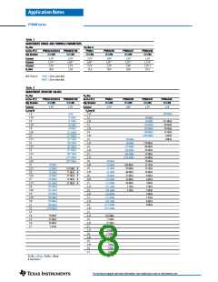
or down using a single external resistor . Table 1 gives the
adjustment range for both Vo1 and Vo2 for each model in
Where: Vo = Original output voltage, (Vo1 or Vo2)
Va = Adjusted output voltage
Rs = The series resistance from Table 1
1
Notes:
1.Use only
a
single 1% resistor in eit(hRer) otrhRe2
1
location to adjust Vo1, and in the (R3) or R4 location to
adjust Vo2. Place the resistor as close to the module as
possible.
the series as Va(min) and Va(max). Note that Vo2 must
2
always be lower than Vo1
.
Vo1 Adjust Up: To increase the output, add a resistor R2
3
between pin 2 (Vo1 Adjust) and pins 7-12 (GND) .
2.Vo 2 must always be at least 0.3V lower than Vo1.
Vo1 Adjust Down: Add a resistor (R1), between pin 2
(Vo1 Adjust) and pin 3 (Vo1 Sense).
3.When adjusting Vohigher than the factory pre-set
1
output voltage the minimum input voltage must be
revised as follows.
Vo2 Adjust Up: Add a resistor R4 between pin 27
(Vo2 Adjust) and pins 17–22 (GND).
Vo1 =3.3V:
Vin(min) = (Vo1 + 1)V or 4.5V, whichever is greater.
Vo2 Adjust Down: Add a resistor (R3) between pin 27
(Vo2 Adjust) and pin 26 (Vo2 Sense).
Vo1 =2.5V:
Vo1 =2.5V is the maximum output voltage allowed for
operation off a 3.3V input bus. If Vo1 is adjusted above
2.5V, the input voltage must be a minimum of 4.5V.
Refer to Figure 1 and Table 2 for both the placement and value of
the required resistor.
4.Vo 1 and Vo2 may be adjusted down to an alternative bus
voltage by making, (R1) or (R3) respectively, a zero ohm
link. Refer to the Table 1 footnotes for guidance.
The adjust up and adjust down resistor values can also be
calculated using the following formulas. Be sure to select
the correct formula parameter from Table 1 for the output
and model being adjusted.
5.Never connect capacitors to either theAdVjuost or
1
Vo2 Adjust pins. Any capacitance added to these control
pins will affect the stability of the respective regulated
output.
10 (Va – 0.9 )
Vo – Va
(R1) or (R3)
=
– Rs
kΩ
9
R2 or R4
=
– Rs
kΩ
Va – Vo
Figure 1
Vo1 Sense
Vo2 Sense
3
26
V1 Sns
V2 Sns
Vo1
4–6
Vo1
Vo2
VIN
13–16
Vin
PT6940
Vo2
23–25
V2 Adj V1 Adj
27
7–12
17–22
2
(R1)
(R3)
+
+
+
CIN
Co1
Co2
L
O
A
D
L
O
A
D
R2
R4
GND
GND
For technical support and more information, see inside back cover or visit www.ti.com

 TI [ TEXAS INSTRUMENTS ]