Application Notes
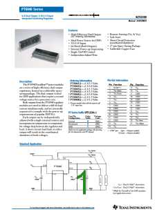
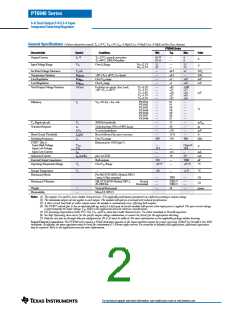
PT6940 Series
Operating Features of the PT6940 Series
of Dual-Output Voltage Regulators
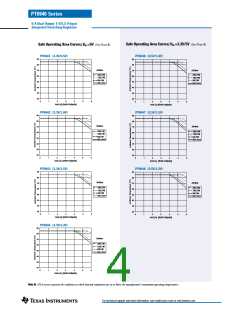
Over-Current Protection
Standby Control
The PT6940 series of regulators incorporate independent
current limit protection at both outputs (Vo1 & Vo2) with a
periodic shutdown of both outputs. Applying a load current,
in excess of the current limit threshold to either output,
results in the shutdown of both voltages after a short
period; typically 15ms. Following shutdown the module
periodically attempts to recover by executing a soft start
power-up at intervals of approximately 100ms. If the over-
current fault persists, each attempted restart will result in a
corresponding over-current trip and shutdown. During
the 15ms period prior to each successive shutdown, the
output with the load fault may not reach full regulation.
The output voltages from the PT6940 may be disabled
using the regulator’s Standby control. The standby function
is provided by the “STBY*” control (pin 1). If pin 1 is left
open-circuit the regulator operates normally, and provides
a regulated output at both Vo1 (pins 4–6) and Vo2 (pins 23–
25) whenever a valid input source voltage is applied to Vin
(pins 13–16) with respect to GND (pins 7-12 & 17–22).
Applying a low-impedance sink to ground1 at pin 1, simul-
taneously disables both regulated outputs. This places the
regulator in standby mode, and reduces the input current
drawn by the ISR to typically 10mA. The Standby control
may also be used to maintain both regulator outputs at zero
volts during the period that input power is applied.
The standby pin is ideally controlled using an open-collector
(or open-drain) discrete transistor (See Figure 2). The
open-circuit voltage is the input voltage, Vin.
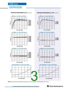
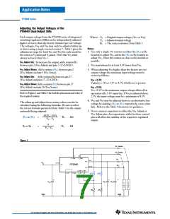
Power-Up Voltage Sequencing
The output voltages from the PT6940 series regulators are
independently regulated, and internally sequenced to meet
the power-up requirements of popular microprocessors
and DSP chipsets. Figure 1 shows the output voltage wave-
forms of a PT6942 (3.3V/1.8V) after either input power is
applied, or the regulator is enabled. In this example turning
Q1 off in Figure 2, removes the low-voltage signal at pin 1
and enables the regulator. Following a delay of about 3–5ms,
Vo1 and Vo2 rise together until the lower voltage, Vo2,
reaches its regulation voltage. Vo1 then continues to rise
until both outputs reach full regulation. The total power-
up time is less than 15ms, and is relatively independent of
load, temperature, and output capacitance. The turn-off of
Q1 corresponds to the rise in VSTBY. The waveforms were
measured with a 5V input voltage, and with resistive loads
of 4A at both the Vo1 and Vo2 outputs.
Figure 2
3
26
V1 Sns
V2 Sns
Vo1
Vo2
4–6
Vo1
Vo2
Vin
13–16
Vin
PT6940
23–25
V2 Adj V1 Adj
17–22 27
STBY*
1
7–12
2
+
+
+
CIN
Co1
Co2
Q1
BSS138
Inhibit
COM
COM
Figure 1
Notes:
1.The standby control inpuNt oitscompatible with TTL or
other devices that incorporate a totem-pole output drive. Use
only a true open-collector device, preferably a discrete bipolar
transistor (or MOSFET). To ensure the regulator output is
disabled, the control pin must be pulled to less than 0.4Vdc
with a low-level 0.5mA sink to ground.
V1 (1V/Div)
V2 (1V/Div)
2
Do not use an an external pull-up resistor. The control pin
has its own internal pull-up. Adding an external pull-up
could disable the over-current protection. The open-circuit
voltage of the “STBY*” pin is the input voltage, Vin.
Vstby (5V/Div)
HORIZ SCALE (2ms/Div)
For technical support and more information, see inside back cover or visit www.ti.com

 TI [ TEXAS INSTRUMENTS ]