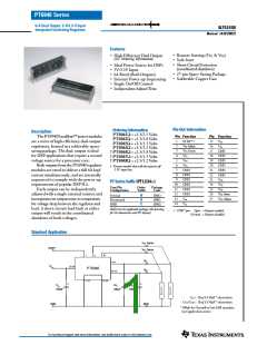
PT6940 Series
6-A Dual Output 5-V/3.3-V Input
Integrated Switching Regulator
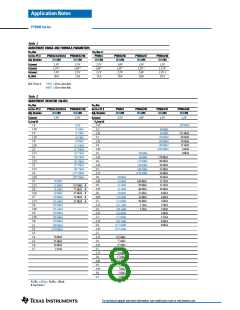
General Specifications (Unless otherwise stated, Ta =25°C, Vin =5V, Cin =330µF, Co1 =330µF, Co2 =330µF, and Io1/Io2 =Iomax)
PT6940 Series
Characteristic
Symbol
Conditions
Min
Typ
Max
Units
(1)
(2)
(2)
OutputCurrent
Io
Ta=25°C,naturalconvection
Ta=60°C,200LFMairflow
0.1
0.1
—
—
6
6
A
Input Voltage Range
Vin
OverIoRange
Vo1 ≤2.5V
3.1
4.5
—
—
5.5
5.5
V
Vo1 >2.5V
Set Point Voltage Tolerance
Temperature Variation
Line Regulation
Vo tol
Regtemp
—
—
—
—
0.5
0.5
5
2
—
10
10
%V
o
%V
o
mV
mV
–40° ≤Ta≤ +85°C, Io =Iomin
Over Vin range
Over Iorange
Reg
line
Load Regulation
Regload
5
Total Output Voltage Variation
∆Votot
Includes set-point, line, load,
Vo =3.3V
Vo =2.5V
Vo =1.8V
Vo =1.5V
Vo =1.2V
—
—
—
—
—
43
35
28
25
22
100
–40° ≤Ta ≤ +85°C
75
54
45
36
mV
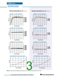
Efficiency
η
Vin =5V, Io1 = Io2 =4A
PT6941
PT6942
PT6943
PT6944
PT6946
PT6947
PT6948
—
—
—
—
—
—
—
92
—
91
90
90
89
88
87
—
—
—
—
—
—
%
Vo Ripple (pk-pk)
TransientResponse
Vr
ttr
∆Vtr
Isc(pk)
ƒo
20MHz bandwidth
1A/µsloadstep, 50%to100%Iomax
Voover/undershoot
Reset followed by auto-recovery
OverVin range
—
—
—
—
35
60
70
13
350
—
—
—
—
mVpp
µs
mV
A
(3)
Short Circuit Threshold
SwitchingFrequency
300
400
kHz
STBY* (Pin 1)
Referencedto GND(pin7)
(4)
Input High Voltage
InputLowVoltage
VIH
VIL
—
—
—
Open
+0.4
V
–0.1
Input Low Current
IIL
Iin standby
—
—
330
–40
-0.5
10
—
–
20
TBD
+85
+125
—
mA
mA
µF
QuiescentCurrent
ExternalOutputCapacitance
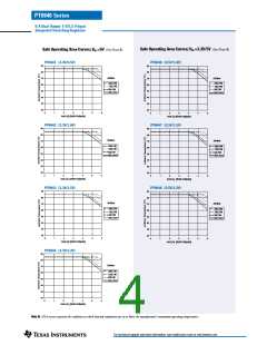
OperatingTemperatureRange
pin 1 to GND
Both outputs
OverVin Range
(5)
(6)
T
a
—
°C
StorageTemperature
Mechanical Shock
T
s
—
–40
—
—
°C
Per Mil-STD-883D, Method 2002.3
1msec, ½Sine, mounted
TBD
G’s
(7)
(7)
Mechanical Vibration
Mil-STD-883D Method 2007.2,
20-2000 Hz
Vertical
—
—
TBD
TBD
—
—
G’s
Horizontal
Weight
Flammability
—
—
Vertical/Horizontal
MeetsUL94V-O
—
34
—
grams
Notes: (1) The outputs, Vo1 and Vo2, have similar characteristics. The applicable performance parameters are defined according to output voltage.
(2) The minimum output current applies to each output. The module will operate at no load with reduced specifications.
(3) A short-circuit load fault at either output causes the module to continuously reset, affecting both outputs.
(4) The STBY* control (pin 1) has an internal pull-up, and if it is left open circuit the module will operate when input power is applied. The open-circuit voltage
is approximately the input voltage, Vin. Refer to the application notes for interface considerations.
(5) For operating temperatures below 0°C, Cin, Co1, and Co2 must have stable characteristics. Use either tantalum or Oscon® capacitors.
(6) See Safe Operating Area curves for the specific output voltage combination, or contact the factory for the appropriate derating.
(7) Only the case pins on through-hole pin configurations (N & A) must be soldered. For more information see the applicable package outline drawing.
Input/O utput Capacitors: The PT6940 series requires a 330µF electrolytic capacitor at the input and both outputs for proper operation (300µF for Oscon® or low ESR
tantalum). In addition, the input capacitance must be rated for a minimum of 1.0Arms ripple current. For transient or dynamic load applications, additional capacitance
may be required. Refer to the application notes for more information.
For technical support and more information, see inside back cover or visit www.ti.com

 TI [ TEXAS INSTRUMENTS ]