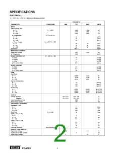
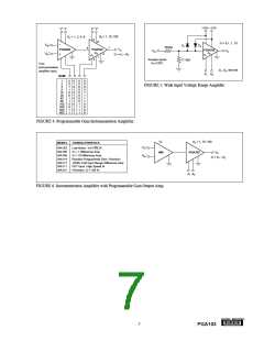
Some applications select gain of the PGA103 with switches
or jumpers. Figure 2 shows pull-up resistors connected to
assure a noise-free logic “1” when the switch or jumper is
off or open. Fixed-gain applications can connect the logic
inputs directly to V+ or ground (or other valid logic level)
without a series resistor.
APPLICATION INFORMATION
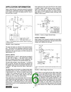
Figure 1 shows the basic connections required for operation
of the PGA103. Applications with noisy or high impedance
power supplies may require decoupling capacitors close to
the device pins as shown.
V+
V–
V+ V–
+15V –15V
0.1µF
0.1µF
8
6
4
7
PGA103
VIN
100kΩ
VO
A
8
0
3
A
1
1
2
6
V+
4
7
100kΩ
VO = G • VIN
PGA103
VIN
3
A0
GAIN
S1
S0
A1
1
1
10
100
Closed Closed
Closed Open
Open Closed
S1
S0
2
Not Valid Open Open
FIGURE 2. Switch or Jumper-Selected Gains.
GAIN
A1
A0
1
10
0
0
1
1
0
1
0
1
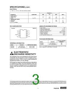
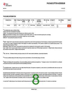
OFFSET TRIMMING
Logic 0: (–5.6) ≤ V ≤ 0.8V
Logic 1: 2V ≤ V ≤ (V+)
Logic voltages referred to pin 3.
100
Offset voltage is laser-trimmed to typically less than 200µV
(referred to input) in all three gains. The input-referred offset
voltage can be different for each gain.
Not Valid
NOTE: (1) Low impedance ground connection required for good gain
accuracy—see text.
FIGURE 1. Basic Connections.
+15V –15V
The input and output are referred to the ground terminal,
pin 3. This must be a low-impedance connection to assure
good gain accuracy. A resistance of 0.1Ω in series with the
ground pin will cause the gain in G=100 to decrease by
approximately 0.2%.
VIN
VO = G (VIN – VTRIM)
PGA103
A0
3
A1
1
VTRIM
2
(1)
+15V
DIGITAL INPUTS
OPA602
±5mV
The digital inputs, A0 and A1, select the gain according to
the logic table in Figure 1. The digital inputs interface
directly to common CMOS and TTL logic components. The
logic inputs are referenced to the ground terminal, pin 3.
100kΩ
50kΩ
Trim Range
33Ω
Logic threshold voltage
is altered by VTRIM
OK for VTRIM ≤ 100mV.
–15V
The logic table in Figure 1 shows that logic “1” on both A0
and A1 is invalid. This logic code will not cause damage, but
the amplifier output will not be predictable while this code
is selected. The output will recover when a valid code is
selected.
.
NOTE: (1) Op amp buffer is required to preserve good gain accuracy—see
text.
The digital inputs are not latched, so a change in logic inputs
immediately selects a new gain. Switching time of the logic
is approximately 0.5µs. The time to respond to gain change
is equal to the switching time plus the time it takes the
amplifier to settle to a new output voltage in the newly
selected gain (see settling time specifications).
FIGURE 3. Offset Voltage Trim Circuit.
Figure 3 shows a circuit used to trim the offset voltage of the
PGA103. An op amp buffers the trim voltage to provide a
low impedance at the ground terminal. This is required to
maintain accurate gain. Remember that the logic inputs, A0
and A1, are referenced to this ground connection, so the
logic threshold voltage will be affected by the trim voltage.
This is insignificant if the offset adjustment is used only to
trim offset voltage. If a large offset is used (greater than
0.1V), be sure that the logic input signals provide valid logic
levels when referred to the voltage at the ground terminal,
pin 3.
Many applications use an external logic latch to access gain
control signals from a high speed data bus. Using an external
latch isolates the high speed digital bus from sensitive
analog circuitry. Locate the latch circuitry as far as practical
from analog circuitry to avoid coupling digital noise into the
analog circuitry.
®
6
PGA103

 TI [ TEXAS INSTRUMENTS ]