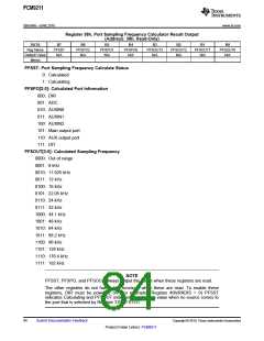
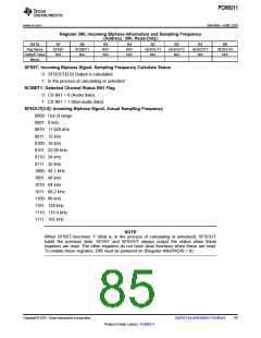
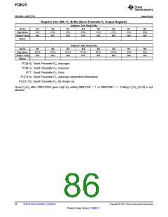
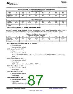
PCM9211
SBAS495 –JUNE 2010
www.ti.com
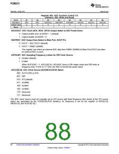
Register 42h, ADC Function Control 1/3
(Address: 42h, Write and Read)
DATA
Reg Name
Default Value
Memo
B7
RSV
0
B6
RSV
0
B5
ADCKOUT
0
B4
ADDTRX7
0
B3
ADFSLMT
0
B2
ADCLK2
0
B1
ADCLK1
1
B0
ADCLK0
0
ADCKOUT: ADC Clock (SCK, BCK, LRCK) Output Select at ADC Power-Down
0: Output enable even at ADDIS = 1 (default)
1: Output disable at ADDIS = 0
ADDTRX7: ADC Output Data Select to Main Port, DOUT Pin
0: DOUT = ADC DOUT (default)
1: DOUT = RXIN7 (ADIN0)
This register can select an external ADC data from RXIN7 (ADIN0) to Main Port DOUT pin when
an external ADC is used.
ADFSLMT: ADC Sampling Frequency Limiter for DIR Clock Source
0: Disable (default)
1: Enable
When ADFSLMT = 1, ADCLK[2:0] = 001(ADC clock is DIR output clock) and DIR locks at
frequency from 14 kHz to 111 kHz, the ADC is forced into power down.
ADCLK[2:0]: ADC Clock Source (SCK/BCK/LRCK) Select
000: AUTO (DIR or XTI)
001: DIR
010: XTI (default)
011: AUXIN0
100: AUXIN1
100: AUXIN2
110: Reserved
111: Reserved
The ADC clock source must be normally set to XTI source with fixed frequency (the clocks at the XTI source
select are generated by the SCK/BCK/LRCK dividers). Its frequency is set by the register of XSCK[1:0],
XBCK[1:0], and XLRCK[1:0].).
88
Submit Documentation Feedback
Copyright © 2010, Texas Instruments Incorporated
Product Folder Link(s): PCM9211

 TI [ TEXAS INSTRUMENTS ]