ꢀ
ꢁ
ꢂ
ꢃ
ꢄ
ꢅ
ꢆ
www.ti.com
SLES080B – MAY 2003 – REVISED NOVEMBER 2003
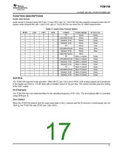
SYSTEM CLOCK AND RESET FUNCTIONS
System Clock Input
The PCM1794 requires a system clock for operating the digital interpolation filters and advanced segment DAC
modulators. The system clock is applied at the SCK input (pin 7). The PCM1794 has a system clock detection circuit
that automatically senses the frequency at which the system clock is operating. Table 1 shows examples of system
clock frequencies for common audio sampling rates.
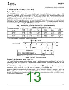
Figure 18 shows the timing requirements for the system clock input. For optimal performance, it is important to use
a clock source with low phase jitter and noise. One of the Texas Instruments PLL1700 family of multiclock generators
is an excellent choice for providing the PCM1794 system clock.
Table 1. System Clock Rates for Common Audio Sampling Frequencies
SYSTEM CLOCK FREQUENCY (F
) (MHz)
512 f
SCK
SAMPLING FREQUENCY
128 f
192 f
256 f
384 f
768 f
S
S
S
S
S
S
32 kHz
44.1 kHz
48 kHz
4.096
5.6488
6.144
6.144
8.4672
9.216
8.192
11.2896
12.288
24.576
49.152
12.288
16.9344
18.432
36.864
73.728
16.384
22.5792
24.576
24.576
33.8688
36.864
96 kHz
12.288
24.576
18.432
36.864
49.152
(1)
73.728
(1)
192 kHz
(1)
This system clock rate is not supported for the given sampling frequency.
t
(SCKH)
H
2.0 V
0.8 V
System Clock (SCK)
L
t
(SCKL)
t
(SCY)
PARAMETERS
MIN
13
(SCY)
0.4t
MAX UNITS
t
System clock pulse cycle time
ns
ns
ns
(SCY)
t
System clock pulse duration, HIGH
System clock pulse duration, LOW
0.4t
(SCY)
(SCKH)
t
(SCKL)
Figure 18. System Clock Input Timing
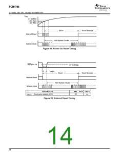
Power-On and External Reset Functions
The PCM1794 includes a power-on reset function. Figure 19 shows the operation of this function. With V
> 2 V,
DD
the power-on reset function is enabled. The initialization sequence requires 1024 system clocks from the time
> 2 V.
V
DD
The PCM1794 also includes an external reset capability using the RST input (pin 14). This allows an external
controller or master reset circuit to force the PCM1794 to initialize to its default reset state.
Figure 20 shows the external reset operation and timing. The RST pin is set to logic 0 for a minimum of 20 ns. The
RST pin is then set to a logic 1 state, thus starting the initialization sequence, which requires 1024 system clock
periods. The external reset is especially useful in applications where there is a delay between the PCM1794 power
up and system clock activation.
13

 TI [ TEXAS INSTRUMENTS ]