RI_OUT Function
RIENB
CSTSMASK
CSC
PC Card
Socket A
RINGEN
Card
I/F
RI_OUT
RI
CDRESUME
PC Card
Socket B
CSC
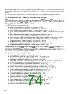
Figure 3−14. RI_OUT Functional Diagram
RI from the 16-bit PC Card interface is masked by bit 7 (RINGEN) in the ExCA interrupt and general control register
(ExCA offset 03h/43h/803h, see Section 5.4). This is programmed on a per-socket basis and is only applicable when
a 16-bit card is powered in the socket.
The CBWAKE signaling to RI_OUT is enabled through the same mask as the CSC event for CSTSCHG. The mask
bit (bit 0, CSTSMASK) is programmed through the socket mask register (CB offset 04h, see Section 6.2) in the
CardBus socket registers.
RI_OUT can be routed through any of three different pins, RI_OUT/PME, MFUNC2, or MFUNC4. The RI_OUT
function is enabled by setting bit 7 (RIENB) in the card control register (PCI offset 91h, see Section 4.38). The PME
function is enabled by setting bit 8 (PME_ENABLE) in the power-management control/status register (PCI offset A4h,
see Section 4.44). When bit 0 (RIMUX) in the system control register (PCI offset 80h, see Section 4.29) is set to 0,
both the RI_OUT function and the PME function are routed to the RI_OUT/PME terminal. If both functions are enabled
and RIMUX is set to 0, then the RI_OUT/PME terminal becomes RI_OUT only and PME assertions are never seen.
Therefore, in a system using both the RI_OUT function and the PME function, RIMUX must be set to 1 and RI_OUT
must be routed to either MFUNC2 or MFUNC4.
3.8.8 PCI Power Management
3.8.8.1 CardBus Power Management (Functions 0 and 1)
The PCI Bus Power Management Interface Specification for PCI to CardBus Bridges establishes the infrastructure
required to let the operating system control the power of PCI functions. This is done by defining a standard PCI
interface and operations to manage the power of PCI functions on the bus. The PCI bus and the PCI functions can
be assigned one of seven power-management states, resulting in varying levels of power savings.
The seven power-management states of PCI functions are:
•
•
•
•
•
•
•
D0-uninitialized − Before controller configuration, controller not fully functional
D0-active − Fully functional state
D1 − Low-power state
D2 − Low-power state
D3 − Low-power state. Transition state before D3
hot
cold
D3
− PME signal-generation capable. Main power is removed and VAUX is available.
cold
D3 − No power and completely nonfunctional
off
NOTE 1: In the D0-uninitialized state, the PCI6x21/PCI6x11 controller does not generate PME and/or interrupts. When bits 0 (IO_EN) and 1
(MEM_EN) of the command register (PCI offset 04h, see Section 4.4) are both set, the PCI6x21/PCI6x11 controller switches the state
to D0-active. Transition from D3
the controller to the D0-uninitialized state immediately.
to the D0-uninitialized state happens at the deassertion of PRST. The assertion of GRST forces
cold
NOTE 2: The PWR_STATE bits (bits 1−0) of the power-management control/status register (PCI offset A4h, see Section 4.44) only code for four
power states, D0, D1, D2, and D3 . The differences between the three D3 states is invisible to the software because the controller
hot
is not accessible in the D3
or D3 state.
off
cold
3−23

 TI [ TEXAS INSTRUMENTS ]