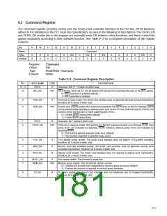
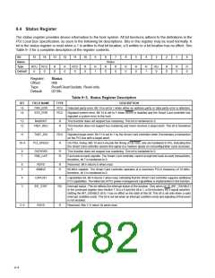
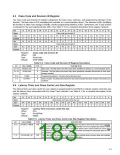
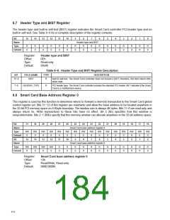
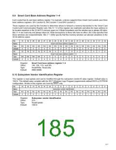
9.9 Smart Card Base Address Register 1−4
Each socket has its own base address register. For example, a device supports three Smart Card sockets uses three
base address registers, BA1 (socket 0), BA2 (socket 1) and BA3 (socket 2).
These registers are used by this function to determine where to forward a memory transaction to the Smart Card
Control and Communication Register sets. Bits 31−12 of this register are read/write and allow the base address to
be located anywhere in the 32-bit PCI memory space on 4-Kbyte boundaries and the window size is always 4K bytes.
Bits 11−4 are read-only and always return 0s. Write transactions to these bits have no effect. Bit 3 (0b) specifies that
these windows are nonprefetchable. Bits 2−1 (00b) specify that this memory window can allocate anywhere in the
32-bit address space.
Bit
31
30
29
28
27
26
25
24
23
22
21
20
19
18
17
16
Name
Type
Default
Bit
Smart Card base address register 1−4
RW
0
RW
0
RW
0
RW
0
RW
0
RW
0
RW
0
RW
0
RW
0
RW
0
RW
0
RW
0
RW
0
RW
0
RW
0
RW
0
15
14
13
12
11
10
9
8
7
6
5
4
3
2
1
0
Name
Type
Default
Smart Card base address register 1−4
RW
0
RW
0
RW
0
RW
0
R
0
R
0
R
0
R
0
R
0
R
0
R
0
R
0
R
0
R
0
R
0
R
0
Register:
Offset:
Type:
Smart Card base address register 1−4
14h, 18h, 1Ch, and 20h
Read/Write, Read-only
0000 0000h
Default:
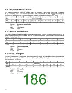
9.10 Subsystem Vendor Identification Register
This register is read-update and can be modified through the subsystem vendor ID alias register. Default value is
104Ch. This default value complies with the WLP (Windows Logo Program) requirements without BIOS or EEPROM
configuration. All bits in this register are reset by GRST only.
Bit
15
14
13
12
11
10
9
8
7
6
5
4
3
2
1
0
Name
Type
Default
Subsystem vendor identification
RU
0
RU
0
RU
0
RU
1
RU
0
RU
0
RU
0
RU
0
RU
0
RU
1
RU
0
RU
0
RU
1
RU
1
RU
0
RU
0
Register:
Offset:
Type:
Subsystem vendor identification
2Ch
Read/Update
104Ch
Default:
9−7

 TI [ TEXAS INSTRUMENTS ]