7 Flash Media Controller Programming Model
This section describes the internal PCI configuration registers used to program the PCI6x21/PCI6x11 flash media
controller interface. All registers are detailed in the same format: a brief description for each register is followed by
the register offset and a bit table describing the reset state for each register.
A bit description table, typically included when the register contains bits of more than one type or purpose, indicates
bit field names, a detailed field description, and field access tags which appear in the type column. Table 4−1
describes the field access tags.
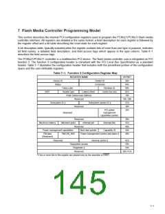
The PCI6x21/PCI6x11 controller is a multifunction PCI device. The flash media controller core is integrated as PCI
function 3. The function 3 configuration header is compliant with the PCI Local Bus Specification as a standard
header. Table 7−1 illustrates the configuration header that includes both the predefined portion of the configuration
space and the user-definable registers.
Table 7−1. Function 3 Configuration Register Map
REGISTER NAME
OFFSET
00h
Device ID
Status
Vendor ID
Command
04h
Class code
Header type
Flash media base address
Revision ID
Cache line size
08h
BIST
Latency timer
0Ch
10h
Reserved
14h−28h
2Ch
Subsystem ID ‡
Subsystem vendor ID ‡
Reserved
30h
PCI power
management
34h
Reserved
capabilities pointer
Reserved
38h
3Ch
40h
44h
48h
Maximum latency
Minimum grant
Reserved
Next item pointer
Interrupt pin
Interrupt line
Capability ID
Power management capabilities
PM data
PMCSR_BSE
Power management control and status ‡
(Reserved)
Reserved
General control ‡
4Ch
50h
Subsystem access
Diagnostic ‡
Reserved
54h
58h−FCh
‡
One or more bits in this register are cleared only by the assertion of GRST.
7−1

 TI [ TEXAS INSTRUMENTS ]