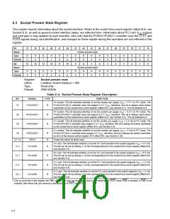
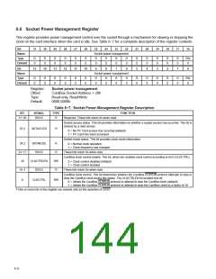
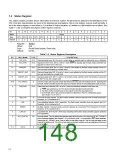
6.6 Socket Power Management Register
This register provides power management control over the socket through a mechanism for slowing or stopping the
clock on the card interface when the card is idle. See Table 6−7 for a complete description of the register contents.
Bit
31
30
29
28
27
26
25
24
23
22
21
20
19
18
17
16
Name
Type
Default
Socket power management
R
0
R
0
R
0
R
0
R
0
R
0
R
0
R
0
R
0
R
0
R
0
R
0
R
0
R
0
R
0
RW
0
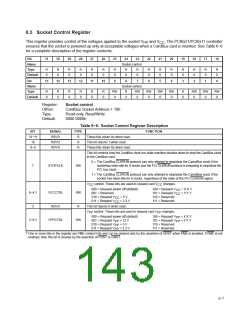
Bit
15
14
13
12
11
10
9
8
7
6
5
4
3
2
1
0
Name
Type
Default
Socket power management
R
0
R
0
R
0
R
0
R
0
R
0
R
0
R
0
R
0
R
0
R
0
R
0
R
0
R
0
R
0
RW
0
Register:
Offset:
Type:
Socket power management
CardBus Socket Address + 20h
Read-only, Read/Write
0000 0000h
Default:
Table 6−7. Socket Power Management Register Description
BIT
SIGNAL
TYPE
FUNCTION
31−26
RSVD
R
Reserved. These bits return 0s when read.
Socket access status. This bit provides information on whether a socket access has occurred. This bit is
cleared by a read access.
25 ‡
SKTACCES
R
0 = No PC Card access has occurred (default).
1 = PC Card has been accessed.
Socket mode status. This bit provides clock mode information.
24 ‡
23−17
16
SKTMODE
RSVD
R
R
0 = Normal clock operation
1 = Clock frequency has changed.
These bits return 0s when read.
CardBus clock control enable. This bit, when set, enables clock control according to bit 0 (CLKCTRL).
CLKCTRLEN
RSVD
RW
R
0 = Clock control disabled (default)
1 = Clock control enabled
15−1
These bits return 0s when read.
CardBus clock control. This bit determines whether the CardBus CLKRUN protocol attempts to stop or
slow the CardBus clock during idle states. The CLKCTRLEN bit enables this bit.
0
CLKCTRL
RW
0 = Allows the CardBus CLKRUN protocol to attempt to stop the CardBus clock (default)
1 = Allows the CardBus CLKRUN protocol to attempt to slow the CardBus clock by a factor of 16
‡
One or more bits in this register are cleared only by the assertion of GRST.
6−8

 TI [ TEXAS INSTRUMENTS ]