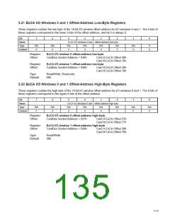
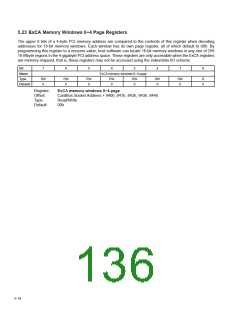
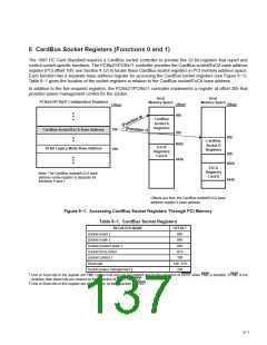
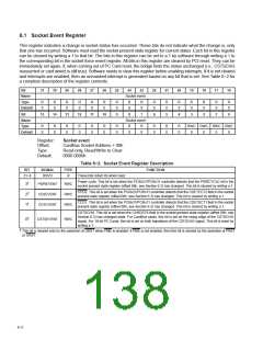
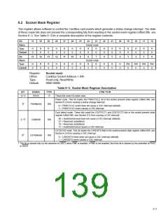
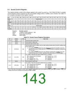
6.2 Socket Mask Register
This register allows software to control the CardBus card events which generate a status change interrupt. The state
of these mask bits does not prevent the corresponding bits from reacting in the socket event register (offset 00h, see
Section 6.1). See Table 6−3 for a complete description of the register contents.
Bit
31
30
29
28
27
26
25
24
23
22
21
20
19
18
17
16
Name
Type
Default
Socket mask
R
0
R
0
R
0
R
0
R
0
R
0
R
0
R
0
R
0
R
0
R
0
R
0
R
0
R
0
R
0
R
0
Bit
15
14
13
12
11
10
9
8
7
6
5
4
3
2
1
0
Name
Type
Default
Socket mask
R
0
R
0
R
0
R
0
R
0
R
0
R
0
R
0
R
0
R
0
R
0
R
0
RW
0
RW
0
RW
0
RW
0
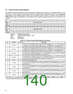
Register:
Offset:
Type:
Socket mask
CardBus Socket Address + 04h
Read-only, Read/Write
0000 0000h
Default:
Table 6−3. Socket Mask Register Description
FUNCTION
BIT
SIGNAL
TYPE
31−4
RSVD
R
These bits return 0s when read.
Power cycle. This bit masks the PWRCYCLE bit in the socket present state register (offset 08h, see
Section 6.3) from causing a status change interrupt.
†
3
PWRMASK
CDMASK
RW
RW
RW
0 = PWRCYCLE event does not cause a CSC interrupt (default).
1 = PWRCYCLE event causes a CSC interrupt.
Card detect mask. These bits mask the CDETECT1 and CDETECT2 bits in the socket present state
register (offset 08h, see Section 6.3) from causing a CSC interrupt.
00 = Insertion/removal does not cause a CSC interrupt (default).
01 = Reserved (undefined)
10 = Reserved (undefined)
†
2−1
11 = Insertion/removal causes a CSC interrupt.
CSTSCHG mask. This bit masks the CARDSTS field in the socket present state register (offset 08h, see
Section 6.3) from causing a CSC interrupt.
†
0
CSTSMASK
0 = CARDSTS event does not cause a CSC interrupt (default).
1 = CARDSTS event causes a CSC interrupt.
†
This bit is cleared only by the assertion of GRST when PME is enabled. If PME is not enabled, then this bit is cleared by the assertion of PRST
or GRST.
6−3

 TI [ TEXAS INSTRUMENTS ]