PCA9306
DUAL BIDIRECTIONAL I2C BUS AND SMBus VOLTAGE-LEVEL TRANSLATOR
www.ti.com
SCPS113–OCTOBER 2004–REVISED APRIL 2005
Absolute Maximum Ratings(1)
over operating free-air temperature range (unless otherwise noted)
MIN
–0.5
–0.5
–0.5
–0.5
MAX
UNIT
VREF1 DC reference voltage range
7
V
VREF2 DC reference bias voltage range
7
7
V
V
VI
Input voltage range(2)
VI/O
Input/output voltage range(2)
Continuous channel current
Input clamp current
7
V
128
–50
220
227
150
mA
mA
IIK
VI < 0
DCT package
DCU package
θJA
Tstg
Package thermal impedance(3)
Storage temperature range
°C/W
°C
–65
(1) Stresses beyond those listed under "absolute maximum ratings" may cause permanent damage to the device. These are stress ratings
only, and functional operation of the device at these or any other conditions beyond those indicated under "recommended operating
conditions" is not implied. Exposure to absolute-maximum-rated conditions for extended periods may affect device reliability.
(2) The input and input/output negative voltage ratings may be exceeded if the input and output current ratings are observed.
(3) The package thermal impedance is calculated in accordance with JESD 51-7.
Recommended Operating Conditions
MIN
0
MAX UNIT
VI/O
Input/output voltage
Reference voltage
SCL1, SDA1, SCL2, SDA2
5
5
V
V
(1)
(1)
VREF1
VREF2
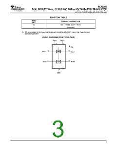
EN
0
Reference voltage
0
5
V
Enable input voltage
Pass switch current
Operating free-air temperature
0
5
V
IPASS
TA
(1)
64
85
mA
°C
–40
V
REF1 ≤ VREF2 – 1 V for best results in level-shifting applications
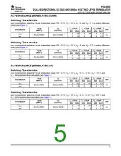
Electrical Characteristics
over recommended operating free-air temperature range (unless otherwise noted)
PARAMETER
Input clamp voltage
Input leakage current
TEST CONDITIONS
EN = 0 V
MIN TYP(1)
MAX UNIT
VIK
IIH
II = –18 mA,
VI = 5 V,
–1.2
5
V
EN = 0 V
µA
pF
pF
pF
Ci(EN) Input capacitance
VI = 3 V or 0
VO = 3 V or 0,
VO = 3 V or 0,
11
4
Cio(off)
Cio(on)
Off capacitance
On capacitance
SCLn, SDAn
SCLn, SDAn
EN = 0 V
EN = 3 V
6
12.5
5.5
7
10.5
3.5
EN = 4.5 V
EN = 3 V
4.7
VI = 0,
IO = 64 mA
IO = 15 mA
EN = 2.3 V
EN = 1.5 V
EN = 4.5 V
EN = 3 V
6.3
9.5
32
(2)
ron
On resistance
SCLn, SDAn
25.5
4.8
Ω
7.5
23
VI = 2.4 V
VI = 1.7 V
14.7
11.3
EN = 2.3 V
16.5
(1) All typical values are at TA = 25°C.
(2) Measured by the voltage drop between the SCL1 and SCL2, or SDA1 and SDA2 terminals, at the indicated current through the switch.
On-state resistance is determined by the lowest voltage of the two terminals.
4

 TI [ TEXAS INSTRUMENTS ]