PCA9306
DUAL BIDIRECTIONAL I2C BUS AND SMBus VOLTAGE-LEVEL TRANSLATOR
www.ti.com
SCPS113–OCTOBER 2004–REVISED APRIL 2005
DESCRIPTION/ORDERING INFORMATION
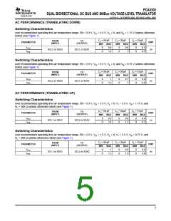
This dual bidirectional I2C and SMBus voltage-level translator, with an enable (EN) input, is operational from
1.2-V to 3.3-V VREF1 and 2.5-V to 5.5-V VREF2
.
The PCA9306 allows bidirectional voltage translations between 1.2 V and 5 V, without the use of a direction pin.
The low ON-state resistance (ron) of the switch allows connections to be made with minimal propagation delay.
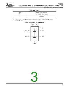
When EN is high, the translator switch is ON, and the SCL1 and SDA1 I/O are connected to the SCL2 and SDA2
I/O, respectively, allowing bidirectional data flow between ports. When EN is low, the translator switch is off, and
a high-impedance state exists between ports.
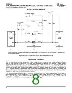
In I2C applications, the bus capacitance limit of 400 pF restricts the number of devices and bus length. Using the
PCA9306 enables the system designer to isolate two halves of a bus; thus, more I2C devices or longer trace
length can be accommodated.
The PCA9306 also can be used to run two buses, one at 400-kHz operating frequency and the other at 100-kHz
operating frequency. If the two buses are operating at different frequencies, the 100-kHz bus must be isolated
when the 400-kHz operation of the other bus is required. If the master is running at 400 kHz, the maximum
system operating frequency may be less than 400 kHz because of the delays added by the repeater.
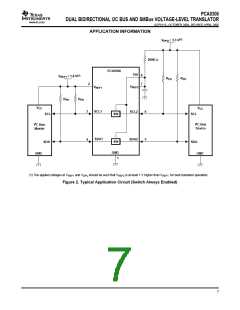
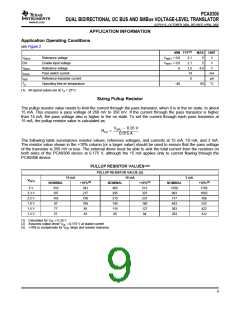
As with the standard I2C system, pullup resistors are required to provide the logic high levels on the translator's
bus. The PCA9306 has a standard open-collector configuration of the I2C bus. The size of these pullup resistors
depends on the system, but each side of the repeater must have a pullup resistor. The device is designed to
work with standard-mode and fast-mode I2C devices, in addition to SMBus devices. Standard-mode I2C devices
only specify 3 mA in a generic I2C system where standard-mode devices and multiple masters are possible.
Under certain conditions, high termination currents can be used.
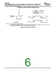
When the SDA1 or SDA2 port is low, the clamp is in the ON state, and a low resistance connection exists
between the SDA1 and SDA2 ports. Assuming the higher voltage is on the SDA2 port when the SDA2 port is
high, the voltage on the SDA1 port is limited to the voltage set by VREF1. When the SDA1 port is high, the SDA2
port is pulled to the drain pullup supply voltage (VDPU) by the pullup resistors. This functionality allows a
seamless translation between higher and lower voltages selected by the user, without the need for directional
control. The SCL1/SCL2 channel also functions as the SDA1/SDA2 channel.
All channels have the same electrical characteristics, and there is minimal deviation from one output to another in
voltage or propagation delay. This is a benefit over discrete transistor voltage translation solutions, since the
fabrication of the switch is symmetrical. The translator provides excellent ESD protection to lower-voltage devices
and at the same time protects less ESD-resistant devices.
ORDERING INFORMATION
TA
PACKAGE(1)
ORDERABLE PART NUMBER
PCA9306DCTR
TOP-SIDE MARKING(2)
7BD_ _ _
Reel of 3000
SSOP – DCT
Reel of 250
Reel of 3000
Reel of 250
PCA9306DCTT
–40°C to 85°C
PCA9306DCUR
VSSOP – DCU
7BD_
PCA9306DCUT
(1) Package drawings, standard packing quantities, thermal data, symbolization, and PCB design guidelines are available at
www.ti.com/sc/package.
(2) DCT: The actual top-side marking has three additional characters that designate the year, month, and assembly/test site.
DCU: The actual top-side marking has one additional character that designates the assembly/test site.
2

 TI [ TEXAS INSTRUMENTS ]