PCA9306
DUAL BIDIRECTIONAL I2C BUS AND SMBus VOLTAGE-LEVEL TRANSLATOR
www.ti.com
SCPS113–OCTOBER 2004–REVISED APRIL 2005
APPLICATION INFORMATION
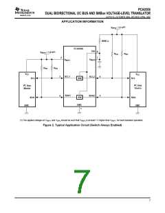
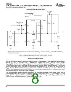
V
DPU
= 3.3 V
(1)
3.3-V Enable Signal
On
Off
200K Ω
PCA9306
EN
(1)
8
7
V
REF1
= 1.8 V
R
PU
R
PU
2
V
V
REF1
REF2
R
PU
R
PU
V
CC
V
CC
3
SCL1
SDA1
SCL2
SDA2
6
5
SCL
SCL
2
SW
SW
2
I C Bus
Device
I C Bus
Master
4
SDA
SDA
GND
1
GND
GND
(1) In the enabled mode, the applied enable voltage and the applied voltage at V
for best translator operation.
should be such that V is at least 1 V higher than V
REF2 REF1
REF1
Figure 3. Typical Application Circuit (Switch Enable Control)
Bidirectional Translation
For the bidirectional clamping configuration (higher voltage to lower voltage or lower voltage to higher voltage),
the EN input must be connected to VREF2 and both pins pulled to high-side VDPU through a pullup resistor
(typically 200 kΩ). This allows VREF2 to regulate the EN input. A filter capacitor on VREF2 is recommended. The
I2C bus master output can be totem pole or open drain (pullup resistors may be required) and the I2C bus device
output can be totem pole or open drain (pullup resistors are required to pull the SCL2 and SDA2 outputs to
VDPU). However, if either output is totem pole, data must be unidirectional or the outputs must be 3-stateable and
be controlled by some direction-control mechanism to prevent high-to-low contentions in either direction. If both
outputs are open drain, no direction control is needed.
The reference supply voltage (VREF1) is connected to the processor core power-supply voltage. When VREF2 is
connected through a 200-kΩ resistor to a 3.3-V to 5.5-V VDPU power supply, and VREF1 is set between 1.0 V and
VDPU – 1 V, the output of each SCL1 and SDA1 has a maximum output voltage equal to VREF1, and the output of
each SCL2 and SDA2 has a maximum output voltage equal to VDPU
.
8

 TI [ TEXAS INSTRUMENTS ]