With the OPA548, the simplest method for adjusting the
current limit uses a resistor or potentiometer connected
between the ILIM pin and V– according to the Equation 1:
APPLICATIONS INFORMATION
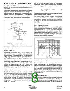
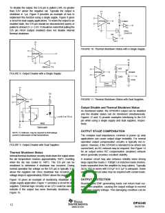
Figure 1 shows the OPA548 connected as a basic noninverting
amplifier. The OPA548 can be used in virtually any op amp
configuration.
15000 4.75
(
)
(
)
– 13750Ω
(1)
RCL
=
Power-supply terminals should be bypassed with low series
impedance capacitors. The technique shown in Figure 7,
using a ceramic and tantalum type in parallel is recom-
mended. In addition, we recommend a 0.01µF capacitor
between V+ and V– as close to the OPA548 as possible.
Power-supply wiring should have low series impedance.
ILIM
The low-level control signal (0µA to 330µA) also allows the
current limit to be digitally controlled.
See Figure 3 for a simplified schematic of the internal
circuitry used to set the current limit. Leaving the ILIM pin
open programs the output current to zero, while connecting
V+
ILIM directly to V– programs the maximum output current limit,
typically 5A.
10µF
R2
R1
+
G = 1+
0.1µF(2)
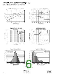
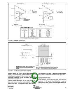
SAFE OPERATING AREA
R1
R2
Stress on the output transistors is determined both by the
output current and by the output voltage across the conduct-
ing output transistor, VS – VO. The power dissipated by the
output transistor is equal to the product of the output current
and the voltage across the conducting transistor, VS – VO.
The Safe Operating Area (SOA curve, Figure 2) shows the
permissible range of voltage and current.
5
E/S
7
2
6
VO
OPA548
VIN
3
ZL
1
(1)
ILIM
4
0.1µF(2)
0.01µF(2)
10µF
+
SAFE OPERATING AREA
10
Current-Limited
V–
NOTES: (1) ILIM connected to V– gives the maximum
TC = 25°C
current limit, 5A (peak). (2) Connect capacitors directly to
package power-supply pins.
P
D
=
5
P
Output current can
be limited to less
than 3A—see text.
0
D
W
=
2
1
6
W
FIGURE 1. Basic Circuit Connections.
P
D
=
1
0
W
POWER SUPPLIES
TC = 85°C
The OPA548 operates from single (+8V to +60V) or dual
(±4V to ±30V) supplies with excellent performance. Most
behavior remains unchanged throughout the full operating
voltage range. Parameters which vary significantly with oper-
ating voltage are shown in the typical characteristic curves.
Pulse Operation Only
(Limit rms current to ≤ 3A)
TC = 125°C
0.1
1
2
5
10
20
50
100
VS
– VO (V)
Some applications do not require equal positive and negative
output voltage swing. Power-supply voltages do not need to
be equal. The OPA548 can operate with as little as 8V
between the supplies and with up to 60V between the
supplies. For example, the positive supply could be set to
55V with the negative supply at –5V, or vice-versa.
FIGURE 2. Safe Operating Area.
The safe output current decreases as VS – VO increases.
Output short-circuits are a very demanding case for SOA. A
short-circuit to ground forces the full power-supply voltage
(V+ or V–) across the conducting transistor. Increasing the
case temperature reduces the safe output current that can be
tolerated without activating the thermal shutdown circuit of
the OPA548. For further insight on SOA, consult Application
Bulletin SBOA022.
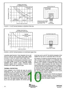
ADJUSTABLE CURRENT LIMIT
The OPA548 features an accurate, user-selected current
limit. Current limit is set from 0A to 5A by controlling the input
to the ILIM pin. Unlike other designs which use a power
resistor in series with the output current path, the OPA548
senses the load indirectly. This allows the current limit to be
set with a 0µA to 330µA control signal. In contrast, other
designs require a limiting resistor to handle the full output
current (5A in this case).
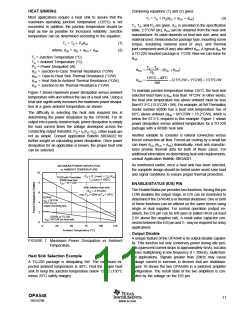
AMPLIFIER MOUNTING
Figure 4 provides recommended solder footprints for both the
TO-220 and DDPAK power packages. The tab of both pack-
ages is electrically connected to the negative supply, V–. It may
be desirable to isolate the tab of the TO-220 package from its
OPA548
8
SBOS070B
www.ti.com

 TI [ TEXAS INSTRUMENTS ]