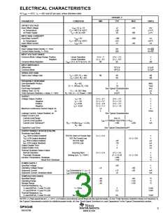
ELECTRICAL CHARACTERISTICS
At TCASE = +25°C, VS = ±30V and E/S pin open, unless otherwise noted.
OPA548T, F
TYP
PARAMETER
CONDITION
MIN
MAX
UNITS
OFFSET VOLTAGE
Input Offset Voltage
vs Temperature
V
CM = 0, IO = 0
A = –40°C to +85°C
VS = ±4V to ±30V
±2
±30
30
±10
mV
µV/°C
µV/V
T
vs Power Supply
100
INPUT BIAS CURRENT(1)
Input Bias Current(2)
vs Temperature
VCM = 0V
–100
±0.5
±5
–500
±50
nA
nA/°C
nA
TA = –40°C to +85°C
CM = 0V
Input Offset Current
V
NOISE
Input Voltage Noise Density, f = 1kHz
Current Noise Density, f = 1kHz
90
200
nV/√Hz
fA/√Hz
INPUT VOLTAGE RANGE
Common-Mode Voltage Range: Positive
Negative
Linear Operation
Linear Operation
CM = (V–) –0.1V to (V+) –3V
(V+) – 3
(V–) – 0.1
80
(V+) – 2.3
(V–) – 0.2
95
V
V
dB
Common-Mode Rejection
V
INPUT IMPEDANCE
Differential
Common-Mode
107 || 6
109 || 4
Ω || pF
Ω || pF
OPEN-LOOP GAIN
Open-Loop Voltage Gain
V
V
O = ±25V, RL = 1kΩ
O = ±25V, RL = 8Ω
90
98
90
dB
dB
FREQUENCY RESPONSE
Gain-Bandwidth Product
Slew Rate
Full-Power Bandwidth
Settling Time: ±0.1%
RL = 8Ω
1
10
MHz
V/µs
kHz
µs
G = 1, 50Vp-p, RL = 8Ω
G = –10, 50V Step
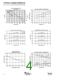
See Typical Characteristics
15
0.02(3)
Total Harmonic Distortion + Noise, f = 1kHz
RL = 8Ω, G = +3, Power = 10W
%
OUTPUT
Voltage Output, Positive
Negative
I
O = 3A
(V+) – 4.1
(V–) + 3.7
(V+) – 2.4
(V–) + 1.3
±3
(V+) – 3.7
(V–) + 3.3
(V+) – 2.1
(V–) + 1.0
V
V
V
V
A
I
O = –3A
IO = 0.6A
O = –0.6A
Positive
Negative
I
Maximum Continuous Current Output: dc
ac
3
Arms
Leakage Current, Output Disabled, dc
Output Current Limit
Current Limit Range
Current Limit Equation
Current Limit Tolerance(1)
See Typical Characteristics
0 to ±5
A
A
mA
I
LIM = (15000)(4.75)/(13750Ω + RCL)
RCL = 14.8kΩ (ILIM = ±2.5A),
RL = 8Ω
±100
±250
Capacitive Load Drive
See Typical Characteristics(4)
OUTPUT ENABLE /STATUS (E/S) PIN
Shutdown Input Mode
VE/S HIGH (output enabled)
E/S Pin Open or Forced High
E/S Pin Forced Low
E/S Pin High
(V–) + 2.4
V
V
µA
µA
µs
µs
V
E/S LOW (output disabled)
IE/S HIGH (output enabled)
E/S LOW (output disabled)
(V–) + 0.8
–65
–70
1
I
E/S Pin Low
Output Disable Time
Output Enable Time
3
Thermal Shutdown Status Output
Normal Operation
Thermally Shutdown
Sourcing 20µA
Sinking 5µA, TJ > 160°C
(V–) + 2.4
(V–) + 3.5
(V–) + 0.35
+160
V
V
°C
°C
(V–) + 0.8
Junction Temperature, Shutdown
Reset from Shutdown
+140
POWER SUPPLY
Specified Voltage
Operating Voltage Range
Quiescent Current
±30
V
V
mA
mA
±4
±30
±20
I
I
LIM Connected to V–, IO = 0
LIM Connected to V–, IO = 0
±17
±6
Quiescent Current, Shutdown Mode
TEMPERATURE RANGE
Specified Range
Operating Range
–40
–40
–55
+85
+125
+125
°C
°C
°C
Storage Range
Thermal Resistance, θJC
7-Lead DDPAK, 7-Lead TO-220
7-Lead DDPAK, 7-Lead TO-220
Thermal Resistance, θJA
7-Lead DDPAK, 7-Lead TO-220
f > 50Hz
dc
2
2.5
°C/W
°C/W
No Heat Sink
65
°C/W
NOTES: (1) High-speed test at TJ = +25°C. (2) Positive conventional current flows into the input terminals. (3) See “Total Harmonic Distortion+Noise vs Frequency” in
the Typical Characteristics section for additional power levels. (4) See “Small-Signal Overshoot vs Load Capacitance” in the Typical Characteristics section.
OPA548
SBOS070B
3
www.ti.com

 TI [ TEXAS INSTRUMENTS ]