OPA171
OPA2171
OPA4171
SBOS516C –SEPTEMBER 2010–REVISED JUNE 2011
www.ti.com
CAPACITIVE LOAD AND STABILITY
or even the output pin. Each of these different pin
functions have electrical stress limits determined by
the voltage breakdown characteristics of the
particular semiconductor fabrication process and
specific circuits connected to the pin. Additionally,
internal electrostatic discharge (ESD) protection is
built into these circuits to protect them from
accidental ESD events both before and during
product assembly.
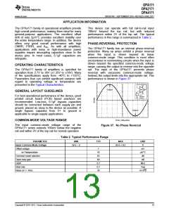
The dynamic characteristics of the OPAx171 have
been optimized for commonly encountered operating
conditions. The combination of low closed-loop gain
and high capacitive loads decreases the phase
margin of the amplifier and can lead to gain peaking
or oscillations. As a result, heavier capacitive loads
must be isolated from the output. The simplest way to
achieve this isolation is to add a small resistor (for
example, ROUT equal to 50Ω) in series with the
output. Figure 38 and Figure 39 illustrate graphs of
small-signal overshoot versus capacitive load for
several values of ROUT. Also, refer to Applications
Bulletin AB-028 (SBOA015), available for download
from the TI website for details of analysis techniques
and application circuits.
These ESD protection diodes also provide in-circuit,
input overdrive protection, as long as the current is
limited to 10mA as stated in the Absolute Maximum
Ratings. Figure 40 shows how a series input resistor
may be added to the driven input to limit the input
current. The added resistor contributes thermal noise
at the amplifier input and its value should be kept to a
minimum in noise-sensitive applications.
50
RL = 10kW
45
40
35
30
25
20
V+
IOVERLOAD
10mA max
VOUT
OPA171
VIN
5kW
G = +1
+18V
ROUT = 0W
15
ROUT
OPA171
Figure 40. Input Current Protection
ROUT = 25W
10
RL
CL
-18V
ROUT = 50W
5
0
An ESD event produces
a
short duration,
high-voltage pulse that is transformed into a short
duration, high-current pulse as it discharges through
a semiconductor device. The ESD protection circuits
are designed to provide a current path around the
operational amplifier core to prevent it from being
damaged. The energy absorbed by the protection
circuitry is then dissipated as heat.
0
100 200 300 400 500 600 700 800 900 1000
Capacitive Load (pF)
Figure 38. Small-Signal Overshoot versus
Capacitive Load (100mV Output Step)
50
ROUT = 0W
45
When the operational amplifier connects into a circuit,
the ESD protection components are intended to
remain inactive and not become involved in the
application circuit operation. However, circumstances
may arise where an applied voltage exceeds the
operating voltage range of a given pin. Should this
condition occur, there is a risk that some of the
internal ESD protection circuits may be biased on,
and conduct current. Any such current flow occurs
through ESD cells and rarely involves the absorption
device.
ROUT = 25W
40
ROUT = 50W
35
30
25
20
RF = 10kW
RI = 10kW
G = -1
15
10
5
+18V
ROUT
OPA171
CL
-18V
0
0
100 200 300 400 500 600 700 800 900 1000
Capacitive Load (pF)
If there is an uncertainty about the ability of the
supply to absorb this current, external zener diodes
may be added to the supply pins. The zener voltage
must be selected such that the diode does not turn
on during normal operation.
Figure 39. Small-Signal Overshoot versus
Capacitive Load (100mV Output Step)
ELECTRICAL OVERSTRESS
However, its zener voltage should be low enough so
that the zener diode conducts if the supply pin begins
to rise above the safe operating supply voltage level.
Designers often ask questions about the capability of
an operational amplifier to withstand electrical
overstress. These questions tend to focus on the
device inputs, but may involve the supply voltage pins
14
Copyright © 2010–2011, Texas Instruments Incorporated

 TI [ TEXAS INSTRUMENTS ]