OPA171
OPA2171
OPA4171
www.ti.com
SBOS516C –SEPTEMBER 2010–REVISED JUNE 2011
APPLICATION INFORMATION
The OPAx171 family of operational amplifiers provide
high overall performance, making them ideal for many
general-purpose applications. The excellent offset
drift of only 2µV/°C provides excellent stability over
the entire temperature range. In addition, the device
offers very good overall performance with high
CMRR, PSRR, and AOL. As with all amplifiers,
applications with noisy or high-impedance power
supplies require decoupling capacitors close to the
device pins. In most cases, 0.1µF capacitors are
adequate.
This device can operate with full rail-to-rail input
100mV beyond the top rail, but with reduced
performance within 2V of the top rail. The typical
performance in this range is summarized in Table 2.
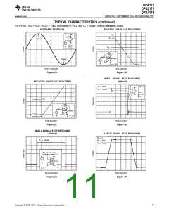
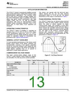
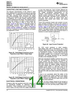
PHASE-REVERSAL PROTECTION
The OPAx171 family has an internal phase-reversal
protection. Many op amps exhibit a phase reversal
when the input is driven beyond its linear
common-mode range. This condition is most often
encountered in noninverting circuits when the input is
driven beyond the specified common-mode voltage
range, causing the output to reverse into the opposite
rail. The input of the OPAx171 prevents phase
reversal with excessive common-mode voltage.
Instead, the output limits into the appropriate rail. This
performance is shown in Figure 37.
OPERATING CHARACTERISTICS
The OPAx171 family of amplifiers is specified for
operation from 2.7V to 36V (±1.35V to ±18V). Many
of the specifications apply from –40°C to +125°C.
Parameters that can exhibit significant variance with
regard to operating voltage or temperature are
presented in the Typical Characteristics.
+18V
OPA171
Output
GENERAL LAYOUT GUIDELINES
-18V
37VPP
For best operational performance of the device, good
printed circuit board (PCB) layout practices are
recommended. Low-loss, 0.1µF bypass capacitors
should be connected between each supply pin and
ground, placed as close to the device as possible. A
single bypass capacitor from V+ to ground is
applicable to single-supply applications.
Sine Wave
(±18.5V)
Output
Time (100ms/div)
COMMON-MODE VOLTAGE RANGE
The input common-mode voltage range of the
OPAx171 series extends 100mV below the negative
rail and within 2V of the top rail for normal operation.
Figure 37. No Phase Reversal
Table 2. Typical Performance Range
PARAMETER
Input Common-Mode Voltage
Offset voltage
MIN
(V+) – 2
TYP
MAX
UNIT
V
(V+) + 0.1
7
mV
vs Temperature
Common-mode rejection
Open-loop gain
12
65
60
0.7
0.7
30
µV/°C
dB
dB
GBW
MHz
V/µs
nV/√Hz
Slew rate
Noise at f = 1kHz
Copyright © 2010–2011, Texas Instruments Incorporated
13

 TI [ TEXAS INSTRUMENTS ]