OPA1611
OPA1612
www.ti.com........................................................................................................................................................ SBOS450A –JULY 2009–REVISED AUGUST 2009
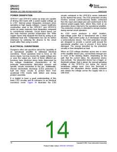
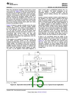
When the operational amplifier connects into a circuit
such as the one Figure 34 shows, the ESD protection
components are intended to remain inactive and not
become involved in the application circuit operation.
However, circumstances may arise where an applied
voltage exceeds the operating voltage range of a
given pin. Should this condition occur, there is a risk
that some of the internal ESD protection circuits may
be biased on, and conduct current. Any such current
flow occurs through steering diode paths and rarely
involves the absorption device.
direct current path is established between the +VS
and –VS supplies. The power dissipation of the
absorption device is quickly exceeded, and the
extreme internal heating destroys the operational
amplifier.
Another common question involves what happens to
the amplifier if an input signal is applied to the input
while the power supplies +VS and/or –VS are at 0V.
Again, it depends on the supply characteristic while at
0V, or at a level below the input signal amplitude. If
the supplies appear as high impedance, then the
operational amplifier supply current may be supplied
by the input source via the current steering diodes.
This state is not a normal bias condition; the amplifier
most likely will not operate normally. If the supplies
are low impedance, then the current through the
steering diodes can become quite high. The current
level depends on the ability of the input source to
deliver current, and any resistance in the input path.
Figure 34 depicts a specific example where the input
voltage, VIN, exceeds the positive supply voltage
(+VS) by 500mV or more. Much of what happens in
the circuit depends on the supply characteristics. If
+VS can sink the current, one of the upper input
steering diodes conducts and directs current to +VS.
Excessively high current levels can flow with
increasingly higher VIN. As a result, the datasheet
specifications recommend that applications limit the
input current to 10mA.
If there is an uncertainty about the ability of the
supply to absorb this current, external zener diodes
may be added to the supply pins as shown in
Figure 34. The zener voltage must be selected such
that the diode does not turn on during normal
operation. However, its zener voltage should be low
enough so that the zener diode conducts if the supply
pin begins to rise above the safe operating supply
voltage level.
If the supply is not capable of sinking the current, VIN
may begin sourcing current to the operational
amplifier, and then take over as the source of positive
supply voltage. The danger in this case is that the
voltage can rise to levels that exceed the operational
amplifier absolute maximum ratings. In extreme but
rare cases, the absorption device triggers on while
+VS and –VS are applied. If this event happens, a
RF
+VS
+V
OPA1611
RI
ESD Current-
Steering Diodes
Out
-In
Op-Amp
Core
+In
Edge-Triggered ESD
Absorption Circuit
RL
ID
(1)
VIN
-V
-VS
(1) VIN = +VS + 500mV.
Figure 34. Equivalent Internal ESD Circuitry and Its Relation to a Typical Circuit Application
Copyright © 2009, Texas Instruments Incorporated
15
Product Folder Link(s): OPA1611 OPA1612

 TI [ TEXAS INSTRUMENTS ]