OPA1611
OPA1612
SBOS450A –JULY 2009–REVISED AUGUST 2009........................................................................................................................................................ www.ti.com
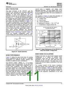
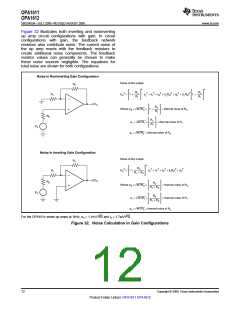
Figure 32 illustrates both inverting and noninverting
op amp circuit configurations with gain. In circuit
configurations with gain, the feedback network
resistors also contribute noise. The current noise of
the op amp reacts with the feedback resistors to
create additional noise components. The feedback
resistor values can generally be chosen to make
these noise sources negligible. The equations for
total noise are shown for both configurations.
Noise in Noninverting Gain Configuration
Noise at the output:
R2
2
2
R2
R1
R2
R1
2
EO
R1
=
1 +
en2 + e12 + e22 + (inR2)2 + eS2 + (inRS)2 1 +
EO
R2
Where eS = Ö4kTRS
e1 = Ö4kTR1
´
= thermal noise of RS
1 +
R1
RS
R2
R1
´
= thermal noise of R1
VS
e2 = Ö4kTR2 = thermal noise of R2
Noise in Inverting Gain Configuration
Noise at the output:
R2
2
R2
2
EO
2
=
1 +
en2 + e12 + e22 + (inR2)2 + eS
R1
R1 + RS
EO
RS
R2
Where eS = Ö4kTRS
´
= thermal noise of RS
= thermal noise of R1
R1 + RS
VS
R2
e1 = Ö4kTR1
´
R1 + RS
e2 = Ö4kTR2 = thermal noise of R2
For the OPA161x series op amps at 1kHz, en = 1.1nV/√Hz and in = 1.7pA/√Hz.
Figure 32. Noise Calculation in Gain Configurations
12
Copyright © 2009, Texas Instruments Incorporated
Product Folder Link(s): OPA1611 OPA1612

 TI [ TEXAS INSTRUMENTS ]