OPA1611
OPA1612
SBOS450A –JULY 2009–REVISED AUGUST 2009........................................................................................................................................................ www.ti.com
POWER DISSIPATION
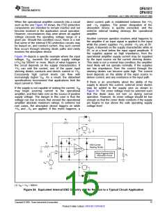
circuits contained in the OPA161x series (indicated
by the dashed line area). The ESD protection circuitry
involves several current-steering diodes connected
from the input and output pins and routed back to the
internal power-supply lines, where they meet at an
absorption device internal to the operational amplifier.
This protection circuitry is intended to remain inactive
during normal circuit operation.
OPA1611 and OPA1612 series op amps are capable
of driving 2kΩ loads with a power-supply voltage up
to ±18V. Internal power dissipation increases when
operating at high supply voltages. Copper leadframe
construction used in the OPA1611 and OPA1612
series op amps improves heat dissipation compared
to conventional materials. Circuit board layout can
also help minimize junction temperature rise. Wide
copper traces help dissipate the heat by acting as an
additional heat sink. Temperature rise can be further
minimized by soldering the devices to the circuit
board rather than using a socket.
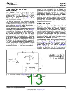
An ESD event produces
a
short duration,
high-voltage pulse that is transformed into a short
duration, high-current pulse as it discharges through
a semiconductor device. The ESD protection circuits
are designed to provide a current path around the
operational amplifier core to prevent it from being
damaged. The energy absorbed by the protection
circuitry is then dissipated as heat.
ELECTRICAL OVERSTRESS
Designers often ask questions about the capability of
an operational amplifier to withstand electrical
overstress. These questions tend to focus on the
device inputs, but may involve the supply voltage pins
or even the output pin. Each of these different pin
functions have electrical stress limits determined by
the voltage breakdown characteristics of the
particular semiconductor fabrication process and
specific circuits connected to the pin. Additionally,
internal electrostatic discharge (ESD) protection is
built into these circuits to protect them from
accidental ESD events both before and during
product assembly.
When an ESD voltage develops across two or more
of the amplifier device pins, current flows through one
or more of the steering diodes. Depending on the
path that the current takes, the absorption device
may activate. The absorption device has a trigger, or
threshold voltage, that is above the normal operating
voltage of the OPA161x but below the device
breakdown voltage level. Once this threshold is
exceeded, the absorption device quickly activates
and clamps the voltage across the supply rails to a
safe level.
It is helpful to have a good understanding of this
basic ESD circuitry and its relevance to an electrical
overstress event. Figure 34 illustrates the ESD
14
Copyright © 2009, Texas Instruments Incorporated
Product Folder Link(s): OPA1611 OPA1612

 TI [ TEXAS INSTRUMENTS ]