OPA1662
OPA1664
SBOS489 –DECEMBER 2011
www.ti.com
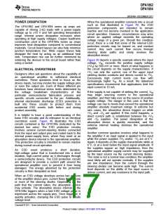
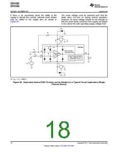
If there is an uncertainty about the ability of the
supply to absorb this current, external zener diodes
may be added to the supply pins as shown in
Figure 48.
The zener voltage must be selected such that the
diode does not turn on during normal operation.
However, its zener voltage should be low enough so
that the zener diode conducts if the supply pin begins
to rise above the safe operating supply voltage level.
TVS
RF
+VS
+V
OPA166x
RI
ESD Current-
Steering Diodes
-In
Out
Op-Amp
Core
RS
+In
Edge-Triggered ESD
Absorption Circuit
RL
ID
(1)
VIN
-V
-VS
TVS
(1) VIN = +VS + 500mV.
Figure 48. Equivalent Internal ESD Circuitry and Its Relation to a Typical Circuit Application (Single
Channel Shown)
18
Copyright © 2011, Texas Instruments Incorporated
Product Folder Link(s): OPA1662 OPA1664

 TI [ TEXAS INSTRUMENTS ]