OPA1662
OPA1664
SBOS489 –DECEMBER 2011
www.ti.com
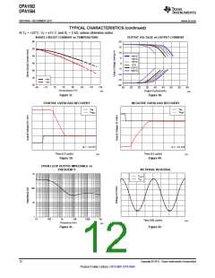
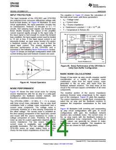
INPUT PROTECTION
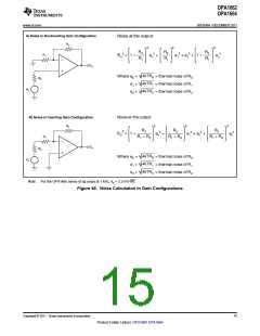
The equation in Figure 45 shows the calculation of
the total circuit noise, with these parameters:
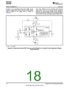
The input terminals of the OPA1662 and OPA1664
are protected from excessive differential voltage with
back-to-back diodes, as Figure 44 illustrates. In most
circuit applications, the input protection circuitry has
no consequence. However, in low-gain or G = +1
circuits, fast ramping input signals can forward bias
these diodes because the output of the amplifier
cannot respond rapidly enough to the input ramp. If
the input signal is fast enough to create this forward
bias condition, the input signal current must be limited
to 10 mA or less. If the input signal current is not
inherently limited, an input series resistor (RI) and/or
a feedback resistor (RF) can be used to limit the
signal input current. This resistor degrades the
low-noise performance of the OPA166x and is
examined in the following Noise Performance section.
Figure 44 shows an example configuration when both
current-limiting input and feeback resistors are used.
•
•
•
•
•
en = Voltage noise
in = Current noise
RS = Source impedance
k = Boltzmann’s constant = 1.38 × 10⁻²³ J/K
T = Temperature in Kelvins (K)
10k
Eo2 = en2 + (inRS)2 + 4KTRS
EO
1k
RS
OPA166x
100
OPA165x
10
Resistor Noise
RF
1
100
1k
10k
100k
1M
G003
Source Resistance (W)
-
Figure 45. Noise Performance of the OPA166x in
Unity-Gain Buffer Configuration
OPA166x
Output
RI
+
Input
BASIC NOISE CALCULATIONS
Design of low-noise op amp circuits requires careful
consideration of
a
variety of possible noise
contributors: noise from the signal source, noise
generated in the op amp, and noise from the
feedback network resistors. The total noise of the
circuit is the root-sum-square combination of all noise
components.
Figure 44. Pulsed Operation
NOISE PERFORMANCE
Figure 45 shows the total circuit noise for varying
source impedances with the op amp in a unity-gain
configuration (no feedback resistor network, and
therefore no additional noise contributions).
The resistive portion of the source impedance
produces thermal noise proportional to the square
root of the resistance. Figure 45 plots this equation.
The source impedance is usually fixed; consequently,
select the op amp and the feedback resistors to
minimize the respective contributions to the total
noise.
The OPA166x (GBW = 22 MHz, G = +1) is shown
with total circuit noise calculated. The op amp itself
contributes both a voltage noise component and a
current noise component. The voltage noise is
commonly modeled as a time-varying component of
the offset voltage. The current noise is modeled as
the time-varying component of the input bias current
and reacts with the source resistance to create a
voltage component of noise. Therefore, the lowest
noise op amp for a given application depends on the
source impedance. For low source impedance,
current noise is negligible, and voltage noise
generally dominates. The low voltage noise of the
OPA166x series op amps makes them a better
choice for low source impedances of less than 1 kΩ.
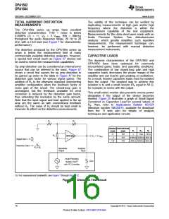
Figure 46 illustrates both inverting and noninverting
op amp circuit configurations with gain. In circuit
configurations with gain, the feedback network
resistors also contribute noise. The current noise of
the op amp reacts with the feedback resistors to
create additional noise components. The feedback
resistor values can generally be chosen to make
these noise sources negligible. The equations for
total noise are shown for both configurations.
14
Copyright © 2011, Texas Instruments Incorporated
Product Folder Link(s): OPA1662 OPA1664

 TI [ TEXAS INSTRUMENTS ]