OPA1662
OPA1664
www.ti.com
SBOS489 –DECEMBER 2011
POWER DISSIPATION
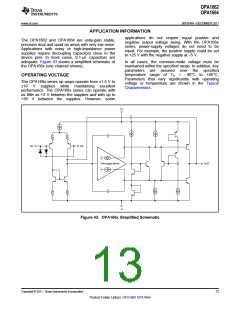
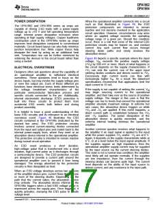
When the operational amplifier connects into a circuit
such as that illustrated in Figure 48, the ESD
protection components are intended to remain
inactive and not become involved in the application
circuit operation. However, circumstances may arise
where an applied voltage exceeds the operating
voltage range of a given pin. Should this condition
occur, there is a risk that some of the internal ESD
protection circuits may be biased on, and conduct
current. Any such current flow occurs through
steering diode paths and rarely involves the
absorption device.
The OPA1662 and OPA1664 series op amps are
capable of driving 2-kΩ loads with a power-supply
voltage up to ±18 V and full operating temperature
range. Internal power dissipation increases when
operating at high supply voltages. Copper leadframe
construction used in the OPA166x series op amps
improves heat dissipation compared to conventional
materials. Circuit board layout can also help minimize
junction temperature rise. Wide copper traces help
dissipate the heat by acting as an additional heat
sink. Temperature rise can be further minimized by
soldering the devices to the circuit board rather than
using a socket.
Figure 48 depicts a specific example where the input
voltage, VIN, exceeds the positive supply voltage
(+VS) by 500 mV or more. Much of what happens in
the circuit depends on the supply characteristics. If
+VS can sink the current, one of the upper input
steering diodes conducts and directs current to +VS.
Excessively high current levels can flow with
increasingly higher VIN. As a result, the datasheet
specifications recommend that applications limit the
input current to 10 mA.
ELECTRICAL OVERSTRESS
Designers often ask questions about the capability of
an operational amplifier to withstand electrical
overstress. These questions tend to focus on the
device inputs, but may involve the supply voltage pins
or even the output pin. Each of these different pin
functions have electrical stress limits determined by
the voltage breakdown characteristics of the
particular semiconductor fabrication process and
specific circuits connected to the pin. Additionally,
internal electrostatic discharge (ESD) protection is
built into these circuits to protect them from
accidental ESD events both before and during
product assembly.
If the supply is not capable of sinking the current, VIN
may begin sourcing current to the operational
amplifier, and then take over as the source of positive
supply voltage. The danger in this case is that the
voltage can rise to levels that exceed the operational
amplifier absolute maximum ratings. In extreme but
rare cases, the absorption device triggers on while
+VS and –VS are applied. If this event happens, a
direct current path is established between the +VS
and –VS supplies. The power dissipation of the
absorption device is quickly exceeded, and the
extreme internal heating destroys the operational
amplifier.
It is helpful to have a good understanding of this
basic ESD circuitry and its relevance to an electrical
overstress event. Figure 48 illustrates the ESD
circuits contained in the OPA166x (indicated by the
dashed line area). The ESD protection circuitry
involves several current-steering diodes connected
from the input and output pins and routed back to the
internal power-supply lines, where they meet at an
absorption device internal to the operational amplifier.
This protection circuitry is intended to remain inactive
during normal circuit operation.
Another common question involves what happens to
the amplifier if an input signal is applied to the input
while the power supplies +VS and/or –VS are at 0 V.
Again, it depends on the supply characteristic while at
0 V, or at a level below the input signal amplitude. If
the supplies appear as high impedance, then the
operational amplifier supply current may be supplied
by the input source via the current steering diodes.
This state is not a normal bias condition; the amplifier
most likely will not operate normally. If the supplies
are low impedance, then the current through the
steering diodes can become quite high. The current
level depends on the ability of the input source to
deliver current, and any resistance in the input path.
An ESD event produces
a
short duration,
high-voltage pulse that is transformed into a short
duration, high-current pulse as it discharges through
a semiconductor device. The ESD protection circuits
are designed to provide a current path around the
operational amplifier core to prevent it from being
damaged. The energy absorbed by the protection
circuitry is then dissipated as heat.
When an ESD voltage develops across two or more
of the amplifier device pins, current flows through one
or more of the steering diodes. Depending on the
path that the current takes, the absorption device
may activate. The absorption device internal to the
OPA166x triggers when a fast ESD voltage pulse is
impressed across the supply pins. Once triggered, it
quickly activates, clamping the ESD pulse to a safe
voltage level.
Copyright © 2011, Texas Instruments Incorporated
17
Product Folder Link(s): OPA1662 OPA1664

 TI [ TEXAS INSTRUMENTS ]