OMAP-L137 Low-Power Applications Processor
SPRS563A–SEPTEMBER 2008–REVISED OCTOBER 2008
www.ti.com
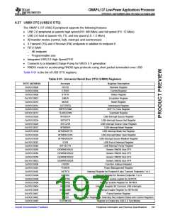
6.26 USB1 Host Controller Registers (USB1.1 OHCI)
All OMAP-L137 USB interfaces are compliant with Universal Serial Bus Specifications, Revision 1.1.
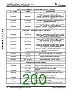
Table 6-89 is the list of USB Host Controller registers.
Table 6-89. USB Host Controller Registers
USB
REGISTER NAME
Register Description
BYTE ADDRESS
0x01E2 5000
0x01E2 5004
0x01E2 5008
0x01E2 500C
0x01E2 5010
0x01E2 5014
0x01E2 5018
0x01E2 501C
0x01E2 5020
0x01E2 5024
0x01E2 5028
0x01E2 502C
0x01E2 5030
0x01E2 5034
0x01E2 5038
0x01E2 503C
0x01E2 5040
0x01E2 5044
0x01E2 5048
0x01E2 504C
0x01E2 5050
0x01E2 5054
0x01E2 5058
HCREVISION
OHCI Revision Number Register
HC Operating Mode Register
HC Command and Status Register
HC Interrupt and Status Register
HC Interrupt Enable Register
HC Interrupt Disable Register
HC HCAA Address Register(1)
HC Current Periodic Register(1)
HC Head Control Register(1)
HC Current Control Register(1)
HC Head Bulk Register(1)
HCCONTROL
HCCOMMANDSTATUS
HCINTERRUPTSTATUS
HCINTERRUPTENABLE
HCINTERRUPTDISABLE
HCHCCA
HCPERIODCURRENTED
HCCONTROLHEADED
HCCONTROLCURRENTED
HCBULKHEADED
HCBULKCURRENTED
HCDONEHEAD
HC Current Bulk Register(1)
HC Head Done Register(1)
HCFMINTERVAL
HC Frame Interval Register
HCFMREMAINING
HCFMNUMBER
HC Frame Remaining Register
HC Frame Number Register
HC Periodic Start Register
HCPERIODICSTART
HCLSTHRESHOLD
HCRHDESCRIPTORA
HCRHDESCRIPTORB
HCRHSTATUS
HC Low-Speed Threshold Register
HC Root Hub A Register
HC Root Hub B Register
HC Root Hub Status Register
HC Port 1 Status and Control Register(2)
HC Port 2 Status and Control Register(3)
HCRHPORTSTATUS1
HCRHPORTSTATUS2
(1) Restrictions apply to the physical addresses used in these registers.
(2) Connected to the integrated USB1.1 phy pins (USB1_DM, USB1_DP).
(3) Although the controller implements two ports, the second port cannot be used.
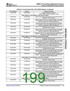
Table 6-90. Switching Characteristics Over Recommended Operating Conditions for USB
LOW SPEED
FULL SPEED
NO.
PARAMETER
UNIT
MIN
MAX
300(1)
300(1)
120(2)
2(1)
MAX
MAX
20(1)
20(1)
110(2)
2(1)
U1
U2
U3
U4
U5
U6
tr
Rise time, USB.DP and USB.DM signals(1)
Fall time, USB.DP and USB.DM signals(1)
Rise/Fall time matching(2)
Output signal cross-over voltage(1)
Differential propagation jitter(3)
Operating frequency(4)
75(1)
75(1)
80(2)
1.3(1)
-25(3)
4(1)
4(1)
90(2)
1.3(1)
-2(3)
ns
ns
tf
tRFM
VCRS
tj
%
V
25(3)
2(3)
ns
fop
1.5
12
MHz
(1) Low Speed: CL = 200 pF. High Speed: CL = 50pF
(2) tRFM =( tr/tf ) x 100
(3) t jr = t px(1) - tpx(0)
(4) fop = 1/tper
196
Peripheral Information and Electrical Specifications
Submit Documentation Feedback

 TI [ TEXAS INSTRUMENTS ]