ꢀ ꢁꢂ ꢂꢃ ꢄ ꢅ ꢀ ꢁꢂ ꢂꢃ ꢄꢆ ꢅ ꢇ ꢆꢂ ꢂ ꢃ ꢄꢅ ꢇ ꢆꢂ ꢂ ꢃ ꢄꢆ
ꢈ ꢉꢆꢊ ꢊ ꢋꢌꢍꢀ ꢋꢎꢇ ꢁ ꢋ ꢏꢁ ꢐꢆꢑꢎ ꢋ ꢀꢆ ꢊ ꢆꢒ ꢏꢊ ꢎꢓ ꢎꢁ ꢐꢇ
SLOS075H − NOVEMBER 1979 − REVISED MAY 2004
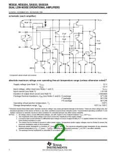
schematic (each amplifier)
V
CC+
36 pF
IN+
37 pF
14 pF
15 Ω
OUT
7 pF
IN−
15 Ω
460 Ω
V
CC−
Component values shown are nominal.
†
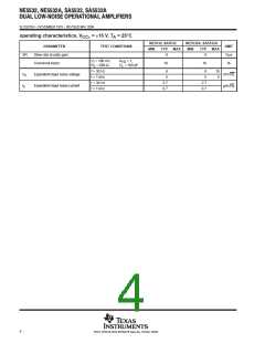
absolute maximum ratings over operating free-air temperature range (unless otherwise noted)ā
Supply voltage (see Note 1): V
V
Input voltage, either input (see Notes 1 and 2) . . . . . . . . . . . . . . . . . . . . . . . . . . . . . . . . . . . . . . . . . . . . . . . . V
. . . . . . . . . . . . . . . . . . . . . . . . . . . . . . . . . . . . . . . . . . . . . . . . . . . . . . . . . . 22 V
. . . . . . . . . . . . . . . . . . . . . . . . . . . . . . . . . . . . . . . . . . . . . . . . . . . . . . . . . −22 V
CC+
CC−
CC
Input current (see Note 3) . . . . . . . . . . . . . . . . . . . . . . . . . . . . . . . . . . . . . . . . . . . . . . . . . . . . . . . . . . . . . . . . 10 mA
Duration of output short circuit (see Note 4) . . . . . . . . . . . . . . . . . . . . . . . . . . . . . . . . . . . . . . . . . . . . . . . Unlimited
Package thermal impedance, θ (see Notes 5 and 6): D package . . . . . . . . . . . . . . . . . . . . . . . . . . . . 97°C/W
JA
P package . . . . . . . . . . . . . . . . . . . . . . . . . . . . 85°C/W
PS package . . . . . . . . . . . . . . . . . . . . . . . . . . . 95°C/W
Operating virtual junction temperature, T . . . . . . . . . . . . . . . . . . . . . . . . . . . . . . . . . . . . . . . . . . . . . . . . . . . 150°C
J
Storage temperature range, T
. . . . . . . . . . . . . . . . . . . . . . . . . . . . . . . . . . . . . . . . . . . . . . . . . . . −65°C to 150°C
stg
†
Stresses beyond those listed under “absolute maximum ratings” may cause permanent damage to the device. These are stress ratings only, and
functional operation of the device at these or any other conditions beyond those indicated under “recommended operating conditions” is not
implied. Exposure to absolute-maximum-rated conditions for extended periods may affect device reliability.
NOTES: 1. All voltage values, except differential voltages, are with respect to the midpoint between V
CC+
and V .
CC−
2. The magnitude of the input voltage must never exceed the magnitude of the supply voltage.
3. Excessive input current will flow if a differential input voltage in excess of approximately 0.6 V is applied between the inputs, unless
some limiting resistance is used.
4. The output may be shorted to ground or either power supply. Temperature and/or supply voltages must be limited to ensure the
maximum dissipation rating is not exceeded.
5. Maximum power dissipation is a function of T (max), θ , and T . The maximum allowable power dissipation at any allowable
J
JA
A
ambient temperature is P = (T (max) − T )/θ . Operating at the absolute maximum T of 150°C can affect reliability.
D
J
A
JA
J
6. The package thermal impedance is calculated in accordance with JESD 51-7.
2
POST OFFICE BOX 655303 • DALLAS, TEXAS 75265

 TI [ TEXAS INSTRUMENTS ]