MSP430G2x53
MSP430G2x13
SLAS735A –APRIL 2011–REVISED MAY 2011
www.ti.com
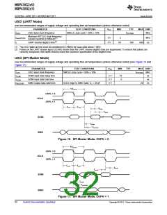
USCI (I2C Mode)
over recommended ranges of supply voltage and operating free-air temperature (unless otherwise noted) (see Figure 20)
PARAMETER
TEST CONDITIONS
VCC
MIN
TYP
MAX UNIT
fSYSTEM MHz
400 kHz
fUSCI
fSCL
USCI input clock frequency
SCL clock frequency
SMCLK, duty cycle = 50% ± 10%
3 V
3 V
0
4.0
0.6
4.7
0.6
0
f
f
f
f
SCL ≤ 100 kHz
SCL > 100 kHz
SCL ≤ 100 kHz
SCL > 100 kHz
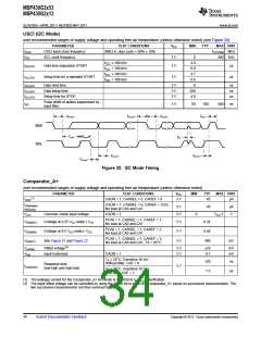
tHD,STA
Hold time (repeated) START
µs
µs
tSU,STA
Setup time for a repeated START
3 V
tHD,DAT
tSU,DAT
tSU,STO
Data hold time
3 V
3 V
3 V
ns
ns
µs
Data setup time
Setup time for STOP
250
4.0
Pulse width of spikes suppressed by
input filter
tSP
3 V
50
100
600
ns
tHD,STA
tSU,STA
tHD,STA
tBUF
SDA
SCL
tLOW
tHIGH
tSP
tSU,DAT
tSU,STO
tHD,DAT
Figure 20. I2C Mode Timing
Comparator_A+
over recommended ranges of supply voltage and operating free-air temperature (unless otherwise noted)
PARAMETER
TEST CONDITIONS
VCC
MIN
TYP
MAX UNIT
(1)
I(DD)
CAON = 1, CARSEL = 0, CAREF = 0
3 V
45
µA
I(Refladder/
RefDiode)
V(IC)
CAON = 1, CARSEL = 0, CAREF = 1/2/3,
No load at CA0 and CA1
3 V
3 V
3 V
45
µA
Common–mode input voltage
CAON = 1
0
VCC-1
V
PCA0 = 1, CARSEL = 1, CAREF = 1,
No load at CA0 and CA1
V(Ref025)
V(Ref050)
V(RefVT)
(Voltage at 0.25 VCC node) / VCC
0.24
0.48
490
PCA0 = 1, CARSEL = 1, CAREF = 2,
No load at CA0 and CA1
(Voltage at 0.5 VCC node) / VCC
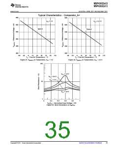
See Figure 21 and Figure 22
3 V
3 V
PCA0 = 1, CARSEL = 1, CAREF = 3,
No load at CA0 and CA1, TA = 85°C
mV
V(offset)
Vhys
Offset voltage(2)
Input hysteresis
3 V
3 V
±10
mV
mV
CAON = 1
0.7
TA = 25°C, Overdrive 10 mV,
Without filter: CAF = 0
120
1.5
ns
Response time
(low-high and high-low)
t(response)
3 V
TA = 25°C, Overdrive 10 mV,
With filter: CAF = 1
µs
(1) The leakage current for the Comparator_A+ terminals is identical to Ilkg(Px.y) specification.
(2) The input offset voltage can be cancelled by using the CAEX bit to invert the Comparator_A+ inputs on successive measurements. The
two successive measurements are then summed together.
34
Submit Documentation Feedback
Copyright © 2011, Texas Instruments Incorporated

 TI [ TEXAS INSTRUMENTS ]